
Step-by-Step Guide to Semiconductor Fab Equipment
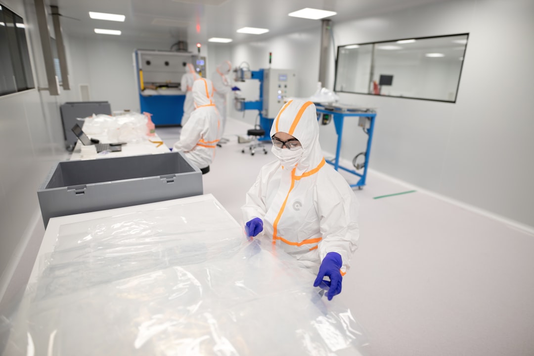
What Is Semiconductor Fab Equipment — And Why It Matters in 2026
Semiconductor fab equipment is every tool, system, and machine used to manufacture chips — from the first layer of silicon all the way to the finished, tested device.
Here’s a quick overview of the main categories:
| Category | What It Does | Examples |
|---|---|---|
| Front-End (Wafer Fab) | Creates circuits on silicon wafers | Lithography, etch, deposition, ion implant |
| Back-End (Assembly & Test) | Packages and tests finished chips | Dicing, wire bonding, flip-chip, burn-in |
| Metrology & Inspection | Measures and detects defects | CD-SEM, optical inspection, overlay tools |
| Automation & Handling | Moves wafers and reticles safely | FOUPs, load ports, vacuum robots, reticle carriers |
The global semiconductor manufacturing equipment market was valued at $166.35 billion in 2025 and is projected to reach $344.36 billion by 2032 — growing at 11% per year. That growth is being driven by AI chips, advanced logic nodes, EV power devices, and a wave of new fab construction across the US, Europe, and Asia.
But here’s something that often gets overlooked in market overviews: none of that equipment works at full potential without protecting the reticles — the photomasks that define every circuit pattern printed on every wafer. A single contaminated or electrostatically damaged reticle can silently corrupt yield across thousands of wafers before anyone detects the problem.
I’m Matt Pilarski, President of Microtome Precision, Inc., the longest-established independent designer and manufacturer of reticle carriers for the semiconductor fab equipment industry, with hands-on experience going back to 1989 — including leading the development of the first SEMI E111-compliant single reticle pod approved by all major lithography OEMs. In this guide, I’ll walk you through every major category of fab equipment, what it does, and where reticle protection fits into the picture.
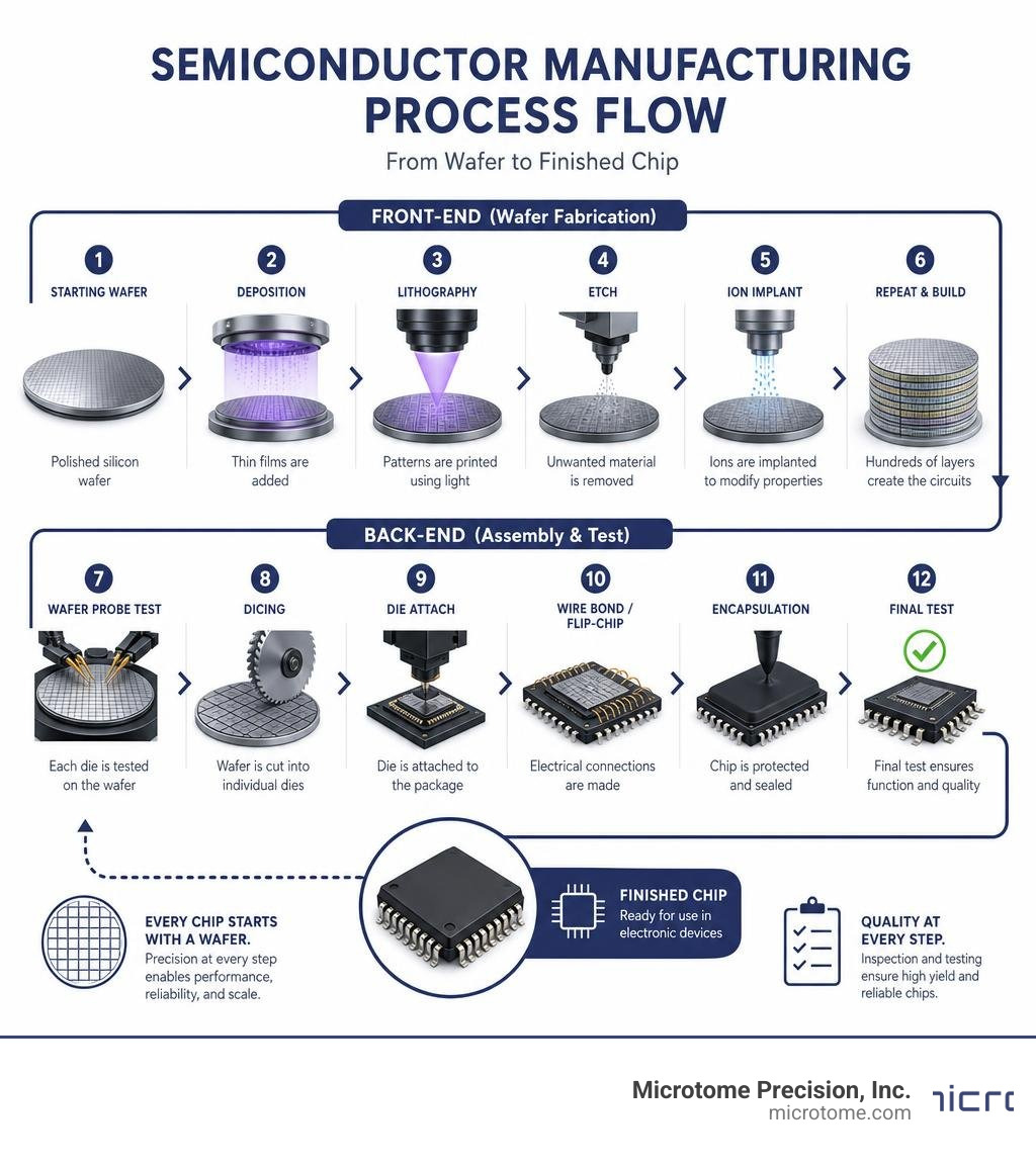
What is Semiconductor Fab Equipment? Front-End vs. Back-End Categories
To understand how microchips are made, we first have to divide the equipment into two main groups: front-end and back-end.
Front-end equipment is where the chemical and physical magic happens. It takes a raw, polished silicon wafer and builds hundreds of layers of microscopic transistors and copper wiring on top of it. Back-end equipment takes that completed wafer, cuts it into individual dies, packages them in protective housings, and tests them to ensure they actually work.
With the market projected to grow to $344.36 billion by 2032, both segments are seeing massive technological leaps. At Microtome Precision, we design solutions that bridge the gap between these phases, ensuring that high-value substrates and photomasks remain pristine as they move from tool to tool. You can explore our full lineup of cleanroom-ready transfer systems in our Products Overview.
Core Front-End Semiconductor Fab Equipment and Process Steps
Front-end fabrication (often called FEOL and BEOL wafer processing) relies on five core physical steps, repeated hundreds of times over a production cycle that averages 11 to 13 weeks (and can stretch up to 15 weeks for advanced nodes):
- Deposition: Adding thin films of insulating or conducting materials onto the wafer. This is done via Chemical Vapor Deposition (CVD), Physical Vapor Deposition (PVD), or Atomic Layer Deposition (ALD) for atomic-scale precision.
- Photolithography: Coating the wafer with a light-sensitive polymer (photoresist) and exposing it to light through a reticle to project the circuit pattern.
- Etching: Removing unprotected areas of the thin film to leave behind the desired pattern. This can be wet chemical etching or dry plasma etching.
- Ion Implantation: Bombarding specific areas of the silicon with dopant ions (like boron or phosphorus) to alter its electrical conductivity and create the semiconductor junctions.
- Chemical Mechanical Planarization (CMP): Using an abrasive slurry and polishing pad to grind the wafer surface perfectly flat before the next layer is deposited.
To see how these steps look in actual hardware, look at vertical diffusion furnaces like the VTR7000PLUS Thermal Reactor | Vertical Diffusion Furnaces – Exper-Tech, which handles high-temperature oxidation and LPCVD steps with a dual-boat automation system to maximize wafer throughput. For precise patterning removal, tools like the MDICP-5000F Fully Automatic ICP Etching Machine / Semiconductor equipment Inductively Coupled Plasma use inductively coupled plasma to etch III-V compounds, silicon, and silicon dioxide with extreme uniformity.
Back-End Assembly, Packaging, and Test Equipment
Once the front-end tools have finished building the transistors and metal lines, the wafer moves to the back-end.
First, the wafer is mounted on tape and cut into individual dies using high-speed dicing saws or lasers. Next, these microscopic dies are attached to a substrate or leadframe. In traditional packaging, thin gold or aluminum wires are bonded from the die to the package pins (wire bonding). In advanced packaging, the die is flipped upside down, and microscopic solder bumps connect it directly to the package substrate (flip-chip).
Advanced packaging has become a major differentiator in 2026. Technologies like 2.5D and 3D chiplets allow multiple separate dies (like a CPU and high-bandwidth memory) to be packaged together on a single silicon interposer. Outsource Semiconductor Assembly and Test (OSAT) companies rely heavily on highly automated pick-and-place systems, molding machines, and advanced testing tools to verify that these complex multi-die packages perform reliably under load.
Global Market Leaders and the Evolution of Wafer Sizes
The semiconductor fab equipment market is one of the most highly consolidated, capital-intensive industries in the world. Historically, three regions have dominated production: the United States, Japan, and the Netherlands. In fact, back in 2016, these three nations held over 90% of the global market share, and that high concentration remains a defining feature of the industry today.
The transition between wafer sizes has also shaped the economics of modern fabs. In the early days of the industry, fabs processed wafers as small as 25 mm (1 inch). Over the decades, the industry standardized on 200 mm (8-inch) and eventually 300 mm (12-inch) wafers.
| Wafer Size | Standard Introduction | Main Applications | Tool Architecture |
|---|---|---|---|
| 200 mm (8″) | 1992 | Power devices, analog, MEMS, RF chips | Open cassettes or SMIF pods; manual/semi-automated |
| 300 mm (12″) | 2000 | Advanced logic (CPU/GPU), DRAM, NAND Flash | FOUPs (Front Opening Unified Pods); 100% automated |
A 300 mm wafer offers more than double the usable surface area of a 200 mm wafer, significantly lowering the manufacturing cost per die. However, upgrading to 300 mm required completely redesigning the equipment to handle the heavier wafers and maintain uniform chemical distribution across a larger surface area.
Top Five Semiconductor Fab Equipment Manufacturers and Market Shares
Today, five massive global corporations collectively command 56% to 66% of the total semiconductor fab equipment market:
- Applied Materials (US): The giant of materials engineering, offering the broadest portfolio of deposition, etch, ion implant, CMP, and metrology tools.
- ASML (Netherlands): The absolute monopoly leader in photolithography, producing the DUV and EUV systems that make modern nanoscale printing possible.
- Lam Research (US): The market leader in etching and critical deposition technologies, particularly essential for building 3D NAND flash memory structures.
- Tokyo Electron (TEL) (Japan): A powerhouse in coater/developers (which work hand-in-hand with lithography tools), etch systems, and thermal processing.
- KLA Corporation (US): The undisputed king of process control, metrology, and defect inspection systems.
Legacy 200 mm vs. Advanced 300 mm Wafer Processing
While advanced logic chips (like those powering your smartphone or AI servers) are built on 300 mm wafers, the demand for legacy 200 mm processing is stronger than ever. The explosion of electric vehicles (EVs), IoT devices, and industrial automation has created a massive need for power semiconductors, analog chips, and MEMS sensors.
Because building a new 300 mm fab is incredibly expensive, many manufacturers use “bridge tools” — equipment that can be converted from 200 mm to 300 mm processing — or build dedicated 200 mm fabs using Standard Mechanical Interface (SMIF) pods to isolate wafers from the environment. At Microtome Precision, we specialize in ensuring tool-to-tool carrier Compatibility across both legacy 200 mm SMIF systems and advanced 300 mm architectures.
Advanced Nodes and the Lithography Revolution: EUV to High-NA EUV
As the industry pushes past 5 nm down to 3 nm, 2 nm, and sub-2 nm “Angstrom” nodes, printing features that are only a few dozen silicon atoms wide has pushed optical physics to its absolute limit.
To put this in perspective: at the 5 nm node, transistor density is incredibly high. For instance, TSMC’s 5 nm process can pack over 170 million transistors into a single square millimeter. Managing defects at this scale is brutally difficult. A test chip with a small die size of 17.92 mm² can achieve a peak yield of over 90%, but as the die size increases to 100 mm² to accommodate larger processors, the yield can drop to around 32% due to the statistical probability of hitting a defect.
To print these ultra-dense patterns without relying on incredibly complex, multi-patterning DUV steps (which require exposing the wafer 4 to 5 times for a single layer), the industry transitioned to Extreme Ultraviolet (EUV) lithography.
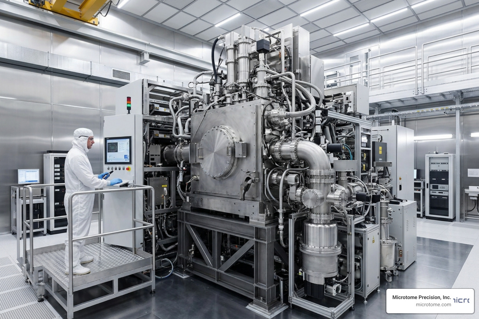
Extreme Ultraviolet (EUV) Lithography Systems in Modern Fabs
EUV lithography represents one of the greatest engineering achievements of the 21st century. While deep ultraviolet (DUV) systems like the TWINSCAN NXT:2050i – DUV lithography machines | ASML use 193 nm immersion optics to print features down to 38 nm, EUV systems drop the light wavelength down to a tiny 13.5 nm.
Because 13.5 nm light is absorbed by almost everything — including cleanroom air and standard glass lenses — the entire optical path must be kept in an extreme high vacuum. Instead of lenses, EUV systems use incredibly precise, multilayer molybdenum/silicon mirrors polished to atomic flatness to bounce and focus the light.
High-volume manufacturing fabs utilize ASML’s NXE platform, which you can read about on the EUV lithography systems – Products | ASML page, to print features down to 13 nm. These machines use a CO2 laser firing 50,000 times per second at microscopic molten tin droplets to generate the EUV light, allowing fabs to simplify process flows, reduce mask count, and cut cycle times.
High-NA EUV and the Future of Sub-2 nm Semiconductor Fab Equipment
To print features below 2 nm, even standard EUV isn’t sharp enough. The industry is now deploying High-Numerical Aperture (High-NA) EUV systems.
By increasing the numerical aperture from 0.33 to 0.55, these next-generation tools can achieve an 8 nm resolution, printing features 1.7 times smaller and enabling a 2.9 times increase in transistor density compared to standard EUV.
The first of these systems, the TWINSCAN EXE:5000 – EUV lithography systems | ASML, introduced anamorphic optics. This design shrinks the pattern by different amounts in the X and Y directions, allowing chipmakers to continue using standard-sized reticles without needing to redesign their entire photomask supply chain. The high-volume production successor, the TWINSCAN EXE:5200B – EUV lithography systems | ASML, is designed to support high-throughput volume manufacturing of sub-2 nm logic and advanced memory nodes, keeping Moore’s Law alive for years to come.
Yield Optimization: Contamination Control, Cleanrooms, and Automation
In a modern semiconductor fab, the air you breathe is a deadly hazard to the wafers. A single speck of dust larger than 10 nanometers can land on a wafer and completely break a transistor, ruining an entire chip.
To prevent this, fabs are built as Class 1 cleanrooms, which use vertical laminar airflow driven by Fan Filter Units (FFUs) to push air straight down through a perforated floor, constantly sweeping particles out of the room.
Wafers themselves are never exposed to the open cleanroom air. Instead, they travel inside sealed plastic pods called FOUPs (Front Opening Unified Pods). These FOUPs are filled with ultra-pure nitrogen or kept under vacuum to prevent copper oxidation and moisture contamination. When a FOUP arrives at a tool, it docks with an Equipment Front End Module (EFEM), which opens the pod doors in an isolated mini-environment, allowing automated wafer handling robots to transfer the wafers into the process chambers.
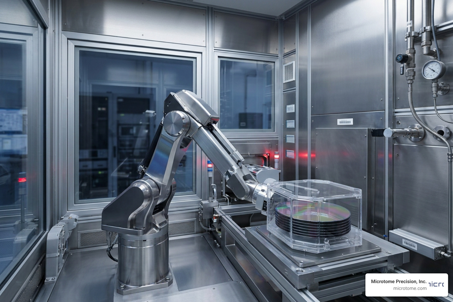
Cleanroom Standards and Vacuum Automation Systems
To maintain high throughput and zero defect rates, advanced fabs are almost entirely automated. Human operators are kept outside the main process bays, and wafers are transported across the ceiling on an Automated Material Handling System (AMHS) of overhead tracks.
Inside the process tools, vacuum automation systems handle the delicate work of moving wafers between load locks and process chambers. Industry leaders like Brooks Automation provide high-reliability vacuum robots (such as the MagnaTran platform) and atmospheric transfer systems (like the Marathon family) that operate for over ten years without maintenance. These robots must move wafers with nanometer-level repeatability while generating absolutely zero particles or vibration, handling up to 50 billion wafer transfers globally every year.
Reticle Protection and Electrostatic Contamination in Semiconductor Fab Equipment
While wafer contamination gets a lot of attention, reticle contamination is actually far more dangerous. If a particle lands on a wafer, you lose one chip. If a particle lands on a reticle, that defect is printed onto every single wafer that passes through the lithography tool, destroying millions of dollars of inventory in a single shift.
Beyond physical particles, reticles face a invisible threat: Electrostatic Field-Induced Migration (EFM). When a reticle is moved, electrostatic charges build up on its surface. These fields attract microscopic airborne polar molecules and particles, pulling them onto the active chrome patterns. Worse, electrostatic discharge (ESD) can instantly melt the microscopic chrome lines on a multi-million-dollar EUV mask.
To solve this, we at Microtome Precision developed our signature all-metal reticle pods, such as the E-Pod Product. Unlike plastic pods that accumulate static charge, our all-aluminum and stainless-steel designs act as a perfect Faraday cage. This completely shields the reticle from external electrostatic fields, preventing EFM and ESD damage during storage and transport.
We also offer an Electrostatic Protection Consultancy Service to help fabs evaluate their tool interfaces and implement SEMI-compliant ESD mitigation strategies across their entire fleet of semiconductor fab equipment.
Geopolitics, Used Equipment Markets, and Future Semiconductor Fab Equipment Trends (2026–2032)
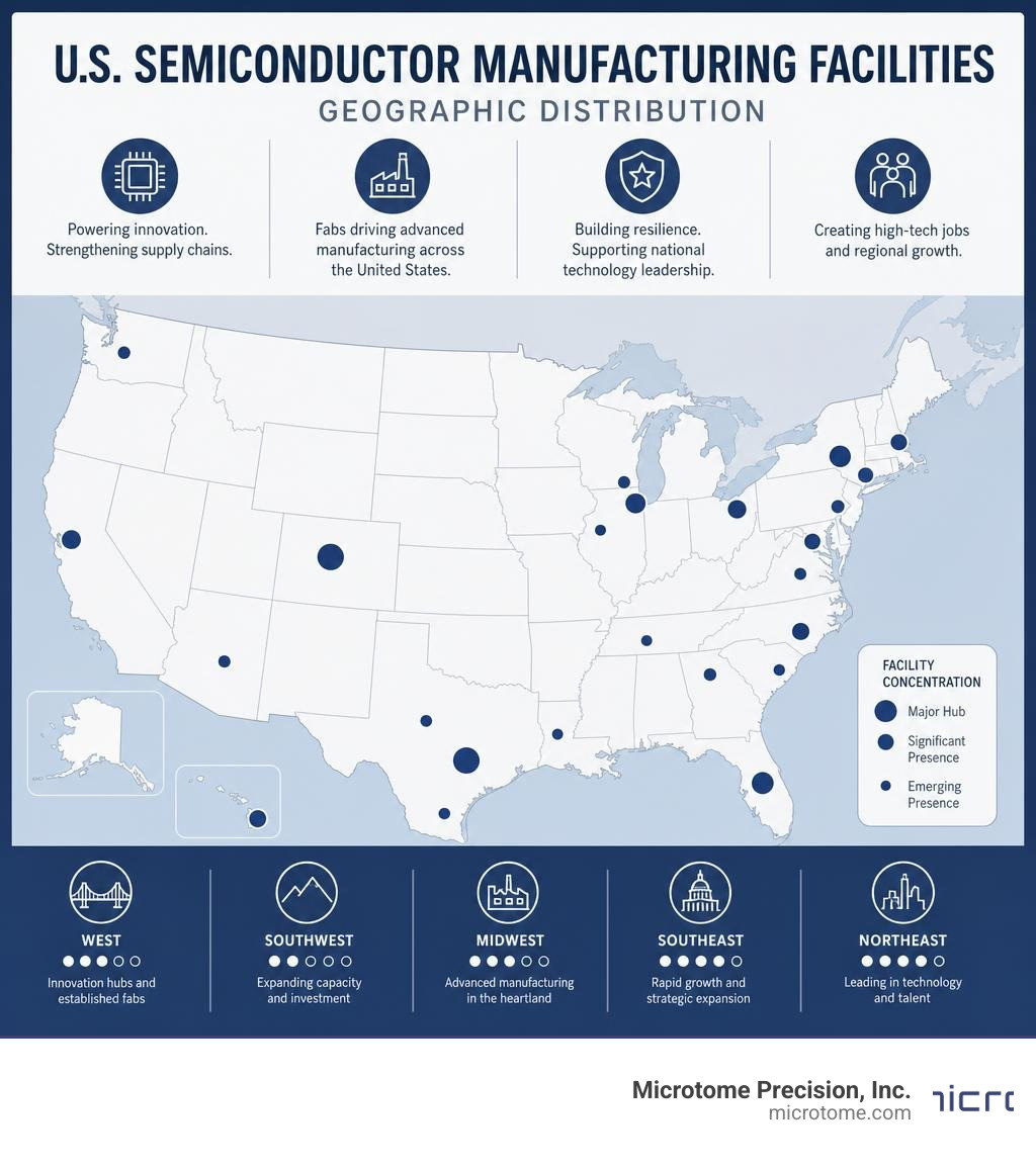
The semiconductor industry is no longer just a commercial market — it is a critical pillar of national security and geopolitical strategy. The passage of the US CHIPS and Science Act and similar European initiatives have kicked off a massive wave of regional investments aimed at localizing supply chains.
Here in Colorado, we are seeing this firsthand. The Colorado Semiconductor Ecosystem has grown into a major hub of advanced manufacturing and R&D. For instance, Microchip Technology announced a massive expansion of its manufacturing center right here in Colorado Springs to boost production of critical automotive and industrial chips, supported by state incentives and federal CHIPS Act funding (detailed on the Growing the Colorado Semiconductor Industry: Microchip to Expand … page).
At the same time, companies like Entegris have broken ground on major manufacturing centers in Colorado Springs to supply the high-purity plastics and filtration systems needed for advanced liquid and gas delivery in fabs, supported by direct CHIPS Act grants (as noted in the Entegris (Colorado) | NIST brief).
These investments are reshaping the U.S. Semiconductor Ecosystem Map, creating highly resilient domestic supply chains that reduce reliance on single-source foreign suppliers.
The Secondary Market for Used and Refurbished Equipment
While multi-billion-dollar megafabs grab the headlines, there is a massive, highly profitable secondary market for used and refurbished semiconductor fab equipment.
Fabs that produce analog, power, and MEMS devices don’t need $150 million High-NA EUV tools; they need reliable, cost-effective 200 mm and legacy 300 mm tools. Original Equipment Manufacturers (OEMs) and specialized refurbishers buy used equipment from consolidating fabs, rebuild them to original specifications, and export them to growing markets in Asia and Europe.
This secondary market is a major driver of trade. Historically, the US semiconductor industry spent an average of $181 million annually on used equipment, allowing legacy fabs to expand capacity quickly and cost-effectively without the long lead times associated with brand-new machinery.
Frequently Asked Questions about Semiconductor Fab Equipment
What is the difference between front-end and back-end semiconductor fab equipment?
Front-end equipment is used to fabricate the actual transistors and metal interconnects on raw silicon wafers (FEOL and BEOL processing). This includes lithography, etching, deposition, and ion implantation. Back-end equipment is used after the wafer is completed to cut it into individual dies, package them in protective housings (like flip-chip or wire-bonded packages), and perform final electrical testing.
Why is EUV lithography so critical for advanced semiconductor fab equipment?
EUV lithography uses a very short 13.5 nm wavelength of light, which allows it to print features down to 13 nm (and 8 nm with High-NA EUV) in a single exposure. Without EUV, fabs would have to use deep ultraviolet (DUV) immersion tools with multiple patterning steps, which adds dozens of extra deposition, etch, and lithography steps, increasing defect rates, cycle times, and manufacturing costs.
How does contamination control impact semiconductor fab equipment yield?
Because modern chip features are measured in nanometers, microscopic dust particles, chemical outgassing, and moisture can easily destroy a circuit. Fabs use Class 1 cleanrooms, laminar airflow, and sealed nitrogen-purged FOUPs to isolate wafers. For reticles, electrostatic charges can attract particles via EFM or cause ESD damage, making Faraday-shielded metal carriers essential for preserving yield.
Conclusion
The world of semiconductor fab equipment is moving faster than ever in 2026. From the deployment of High-NA EUV systems to the massive expansion of legacy 200 mm fabs for the EV market, the demands on equipment reliability, automation, and contamination control have never been higher.
As fabs continue to scale down to the Angstrom era, protecting the photomasks that hold your intellectual property is a critical step in securing your yield. Since 1989, Microtome Precision, Inc. has been at the forefront of this mission, designing all-metal reticle pods that offer unparalleled Faraday-cage protection against EFM and ESD damage.
Whether you need custom carrier designs, compatibility testing for legacy tools, or expert support, we are here to help. Explore our Support and Repair services or Contact Us today to discuss how we can protect your yield in the modern fab environment.