
A Comprehensive Guide to Advanced Reticle Packaging

Why Advanced Reticle Packaging Defines the Future of High-Performance Computing
Advanced reticle packaging sits at the center of one of the most critical challenges in modern semiconductor manufacturing: how do you connect multiple chiplets, memory stacks, and logic dies into a single, reliable package when the laws of physics — and the limits of lithography equipment — stand in the way?
Here is a quick answer to what advanced reticle packaging means and why it matters:
| Concept | Plain-language explanation |
|---|---|
| Reticle limit | A lithography scanner can only expose a fixed area (~700 mm²) in one shot — this is the reticle field |
| Reticle stitching | Exposing a wafer multiple times side-by-side to create dies or interposers larger than one reticle field |
| Silicon interposer | A silicon substrate that connects multiple chiplets — often requires stitching across 2–3+ reticle fields |
| Bridge-based packaging | Small silicon bridges embedded in organic substrates to connect chiplets locally, avoiding large interposers |
| Panel-level packaging | Manufacturing interposers or fan-out packages on large rectangular panels instead of round wafers |
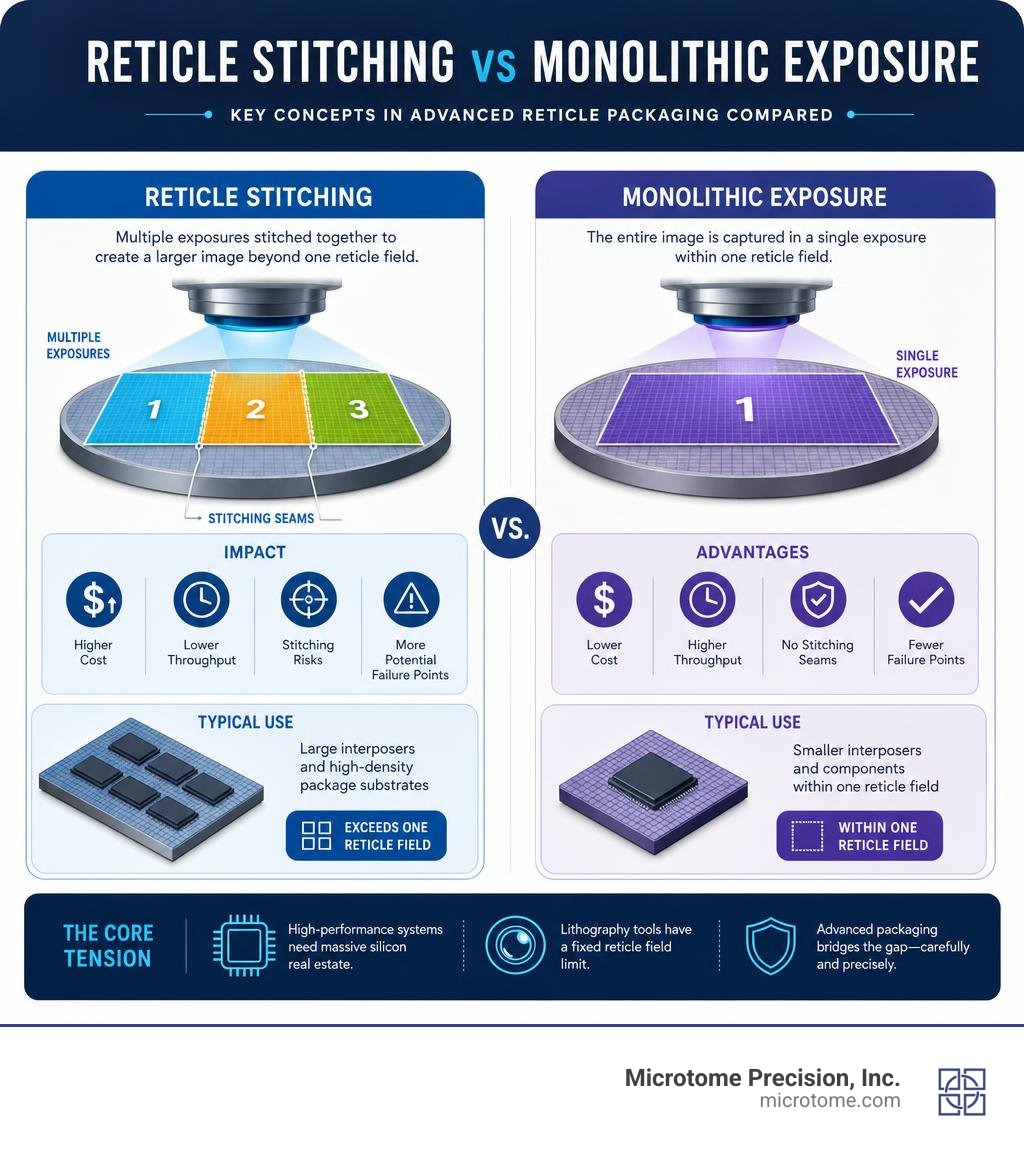
The core tension is straightforward. AI accelerators and HPC systems need massive silicon real estate. But lithography scanners — the machines that print circuit patterns — are physically limited in how large a single exposure can be. TSMC’s current silicon interposer limit sits at 3.3X the reticle size, with roadmaps pushing toward 12X or beyond. Every time an interposer exceeds that single-shot boundary, manufacturers must stitch multiple exposures together — adding cost, reducing throughput, and introducing new failure modes at every seam.
At the same time, the reticles themselves — the glass photomasks that carry the circuit patterns into those scanners — are high-value, fragile assets. A single production reticle can cost over a million dollars and take weeks to qualify. Protecting them from contamination, mechanical damage, and electrostatic hazards like EFM (Electric Field induced Migration) is a discipline entirely its own, and one that becomes more critical as package complexity grows.
I’m Matt Pilarski, President of Microtome Precision, Inc., the longest-established independent designer and manufacturer of reticle carriers in the semiconductor industry — with more than three decades focused specifically on advanced reticle packaging protection, SEMI standards compliance, and EFM prevention. In this guide, I’ll walk through the full landscape: from the mechanics of reticle stitching and interposer design, to the carrier standards and electrostatic safeguards that keep the reticles themselves safe throughout the process.
Lithography Constraints and the Mechanics of Reticle Stitching
To understand why advanced reticle packaging is so challenging, we must first look at the lithography step. Lithography is generally the most expensive process on the wafer, taking up approximately 50% of the manufacturing cost in standard CMOS fabrication. When we build silicon interposers—the silicon foundations used to route signals between chiplets—we are essentially using CMOS-type fabrication but on a different scale, complete with through-silicon vias (TSVs) and fine-pitch metal layers.
Because interposers feature relatively larger metal lines and spaces compared to the sub-2nm features on advanced logic dies, we do not need the most expensive EUV scanners to print them. Instead, we typically rely on older, more cost-effective lithography nodes, such as 248nm or 365nm (i-line) wavelengths.
However, even legacy scanners are bound by the standard reticle field limit (typically 33 mm x 26 mm, or roughly 858 mm²). If we need to build an interposer that is 2X, 3.X, or even 4X this size to accommodate an AI GPU and eight stacks of High Bandwidth Memory (HBM), we cannot print it in a single exposure. We must use a technique called reticle stitching.
In reticle stitching, the wafer stage moves precisely between exposures so that adjacent reticle patterns are printed side-by-side on the wafer. Unlike double patterning—which overlays two exposures on top of each other to resolve finer features—stitching requires a physical overlap region at the boundary of adjacent exposures. This overlap region ensures that the metal lines running from one exposure field to the next connect seamlessly.
Achieving this continuity is highly complex. The scanner’s alignment tolerance and overlay accuracy must be managed to prevent open circuits or high-resistance bottlenecks at the stitching boundary. Furthermore, variations in film thickness across these large areas can cause severe defects during subsequent processing steps.
To overcome this, advanced packaging lines employ process optimizations like the Embedded Trace RDL (ETR) process described in S-SWIFT Packaging with Fine Pitch Embedded Trace RDL – Amkor Technology. By implementing extreme uniform coating techniques, engineers can reduce film thickness variation across the wafer from 0.47 μm down to 0.12 μm. This uniformity is crucial for subsequent chemical mechanical planarization (CMP) steps, preventing “shadowing” or over-etching at the stitched boundaries.
Alignment Tolerances and Interconnect Continuity
The margin for error at a stitched boundary is incredibly small. Modern interposers feature sub-micron routing, where even a minor overlay error can break the conductive pathways. If the scanner’s alignment shifts by even a fraction of a micron, the metal traces printed in “Shot A” will not line up with those in “Shot B.”
To mitigate this, design rules specify exact overlap parameters. As documented in SCALABLE PACKAGE ARCHITECTURE USING RETICLE STITCHING AND PHOTONICS FOR ZETTA-SCALE INTEGRATED CIRCUITS – Patent Application, we can program the lithographic equipment to select individual fields using mechanical blading, leaving a slight overlap (such as 0.5 microns) between stitched fields to guarantee electrical connectivity. Furthermore, by routing conductive pathways through what would normally be the scribe regions (the sacrificial areas where wafers are diced), we can allow adjacent circuits on a single massive die to communicate with high-density interconnects having a pitch of 10 micrometers or less. This approach enables high-bandwidth communication across stitched boundaries without the need for discrete physical bridge dies.
Process Optimization and Yield Dynamics
Even when alignment is perfect, chemical and physical variations during wafer processing can destroy yield. When polishing copper interconnects on stitched interposers, over-polishing can cause “dishing”—where the copper in wide trenches is eroded faster than the surrounding dielectric. To prevent this, we implement a CMP stop layer to limit the maximum dishing depth to approximately 90 nm.
Additionally, we must carefully select dielectric materials and process conditions to prevent copper ion migration. This is especially critical under high-temperature, high-humidity bias testing (such as BHAST), where moisture absorption in organic dielectrics can lead to dendritic copper growth and short circuits.
To model, verify, and enforce these complex physical and electrical design rules across stitched boundaries, package designers rely on highly sophisticated software. Tools such as those detailed in the Allegro X Advanced Package Designer Datasheet | Cadence allow engineers to perform constraint-driven physical layouts, 3D wirebond clearance checking, and early power-delivery network (PDN) analysis. This level of modeling is essential to ensure that the physical boundaries of reticle stitching do not introduce unexpected signal or power integrity issues.
Advanced Reticle Packaging: Overcoming Physical Size Limits in 2.5D and 3D Architectures
As we look at the physical layout of modern high-performance systems, the limits of monolithic silicon are clear. To package next-generation AI accelerators, we must integrate multiple logic dies and HBM stacks. This requirement has driven the evolution of TSMC’s Chip-on-Wafer-on-Substrate (CoWoS) platform, which is categorized into three primary variants:
- CoWoS-S (Silicon Interposer): This classic 2.5D configuration utilizes a full silicon interposer with high-density interconnects and integrated stand-alone embedded deep trench capacitors (eDTCs) underneath the active logic dies. It currently supports interposer sizes up to 3.3X the standard reticle size (~2700 mm²).
- CoWoS-R (RDL Interposer): This variant replaces the silicon interposer with a flexible polymer-based Redistribution Layer (RDL) interposer, offering a minimum routing pitch of 4 μm. This helps buffer the Coefficient of Thermal Expansion (CTE) mismatch between the silicon dies and the organic substrate, reducing package warpage.
- CoWoS-L (Local Silicon Interconnect): Combining the best of both worlds, CoWoS-L embeds small, high-density Local Silicon Interconnect (LSI) bridges inside an organic RDL-based interposer. This allows sub-micron routing only where it is needed (die-to-die boundaries), while utilizing cheaper organic materials elsewhere.

Fabricating the reticles required for these ultra-large interposers demands exceptional mask-making precision. Photomask manufacturers use advanced binary reticles and specialty phase-shift masks, such as those discussed by Advanced Binary Reticle – Photronics Inc, to achieve the required resolution and depth of focus (DOF). These masks utilize technologies like 6% transmission MoSiON absorbers to introduce a 180-degree phase shift, allowing clean patterning of fine features down to the 10nm node and below.
The Role of Advanced Reticle Packaging in Heterogeneous Integration
While full-size stitched silicon interposers deliver exceptional signal performance, they suffer from poor wafer utilization. For extremely large packages (greater than 8X reticle size), wafer utilization can drop to as low as 60% due to the circular geometry of the wafer and the square shape of the interposers.
To solve this, alternative architectures like Intel Foundry’s Embedded Multi-die Interconnect Bridge (EMIB) have gained massive traction. EMIB-T (and its 3D counterpart, EMIB 3.5D) bypasses the full-size silicon interposer entirely. Instead, small silicon bridges are embedded directly into an organic package substrate.
This localized approach delivers superior silicon efficiency, achieving approximately 90% wafer utilization for the small silicon bridges. EMIB-T currently enables systems with a total area exceeding 6X the reticle size, with roadmaps scaling past 12X by 2028, accommodating more than 16 HBM4/HBM5 stacks using upwards of 30 embedded bridges.
Looking further out, some patent applications, such as METHODS AND SYSTEM FOR ADDITIVE MANUFACTURED SEMICONDUCTOR PACKAGING, ASSEMBLIES, AND HETEROGENEOUS INTEGRATION | TREA, propose moving beyond planar constraints entirely. These approaches explore three-dimensional additive manufacturing techniques, introducing “volume distribution layers” (VDL) and “volume interface bridges” (VIB) to route signals in three dimensions, potentially bypassing traditional lithography-based interposers altogether for specialized, flexible, or non-planar form factors.
Contamination Control and Carrier Standards for Advanced Reticle Packaging
As package sizes grow and reticle stitching becomes standard, the reticles themselves are exposed to longer runtimes inside lithography tools. This extended exposure makes them highly vulnerable to defect-causing hazards. In advanced lithography, reticle carriers must comply with strict SEMI standards:
- SEMI E111: Specifies the standards for a single reticle Standard Mechanical Interface (SMIF) pod.
- SEMI E112: Defines the standards for multi-reticle cassettes and pods used for transporting and storing multiple masks.
At Microtome Precision, Inc., based in Colorado Springs, Colorado, we have spent decades researching how to keep these vital assets safe. One of our core findings is that conventional cleanroom ESD (Electrostatic Discharge) countermeasures can actually increase the risk of damage to reticles.
While air ionizers, static-dissipative plastics, and grounded ESD mats work well for standard wafer handling, they are inadequate—and often dangerous—for reticles. This is because the dominant electrostatic risk to a photomask is not a high-voltage ESD spark, but EFM (Electric Field induced Migration).
Discovered through our proprietary research in 2003, EFM occurs at incredibly low electrostatic field strengths. When an electric field is present, sub-micron airborne particles are polarized and actively pulled onto the reticle surface, bypassing cleanroom airflow. Furthermore, these fields can cause chrome migration across the quartz substrate, ruining the mask’s optical properties.
Static-dissipative or “conductive” plastics do not block electric fields; they merely leak charge slowly. To truly protect a reticle from EFM, it must be housed in a complete, all-metal Faraday cage. Our all-metal SMIF pods and cassettes provide absolute electric-field shielding, ensuring that external electrostatic fields cannot penetrate the carrier. To help fabs identify and eliminate these hidden risks, we offer a specialized Electrostatic Protection Consultancy Service to audit cleanroom environments and reticle handling flows.
Comparing Interposer Technologies, Silicon Bridges, and Panel-Level Flows
When designing a high-performance package, engineering teams must weigh the trade-offs between full silicon interposers, organic interposers with embedded bridges, and emerging panel-level flows. Each approach has distinct profiles regarding signal performance, warpage, assembly yield, and manufacturing cost.
| Metric | Silicon Interposer (e.g., CoWoS-S) | Organic Interposer with Bridges (e.g., EMIB, CoWoS-L) | Panel-Level Packaging (PLP) |
|---|---|---|---|
| Signal Performance | Excellent (sub-micron line/space) | High (localized to the bridge area) | Moderate to High (rapidly improving) |
| Warpage Control | Poor (high CTE mismatch with organic substrate) | Good (organic substrate absorbs stress) | Challenging (large area polymer curing) |
| Assembly Yield | Moderate (impacted by large-area stitching defects) | High (only small bridges are silicon) | Developing (highly dependent on die-shift correction) |
| Wafer/Panel Utilization | Low (~60% for large form factors) | High (~90% for silicon bridge dies) | Outstanding (rectangular format eliminates edge waste) |
| Relative Cost | High | Moderate | Low (at high volume) |
To combat the high cost of wafer-based manufacturing, the industry is actively developing Panel-Level Packaging (PLP) technologies. Rather than processing circular 300mm silicon wafers, PLP processes large, rectangular organic panels (typically 18″ x 24″ or 610mm x 457mm).
As discussed in High Density RDL Technologies for Panel Level Packaging of Embedded Dies, one of the primary technical hurdles in PLP is “die shift.” When chiplets are embedded into an organic panel, the polymer materials shrink and expand during curing, causing the dies to shift or rotate slightly from their nominal positions.
To resolve this, advanced PLP lines use adaptive imaging. After the dies are embedded, automated optical systems measure the exact coordinates of every single chiplet on the panel. The direct-write lithography system then dynamically recalculates and adapts the RDL routing pattern in real-time for each unique panel. Combined with thin physical vapor deposition (PVD) seed layers (less than 100nm of Ti/Cu) and dry etching, this adaptive patterning enables reliable 5 μm line and space routing across massive panel areas.
Equipment Innovations and Throughput Scaling
To make large-scale advanced reticle packaging economically viable, equipment manufacturers are introducing several key hardware innovations:
- Multi-Reticle Stage Scanners: Scanners equipped with two wafer stages and a single, high-speed reticle stage allow the tool to switch between different mask patterns rapidly, reducing the overhead of reticle stitching.
- Changes in Reduction Ratios: While standard scanners use a 4:1 reduction ratio, moving to different ratios or utilizing larger reticle formats (such as 6×12 inch reticles) can double the single-shot exposure field, eliminating the need for stitching on mid-sized packages.
- Panel-Based Flows: Transitioning from step-and-repeat wafer steppers to high-throughput, large-field direct imaging systems designed specifically for rectangular panel formats.
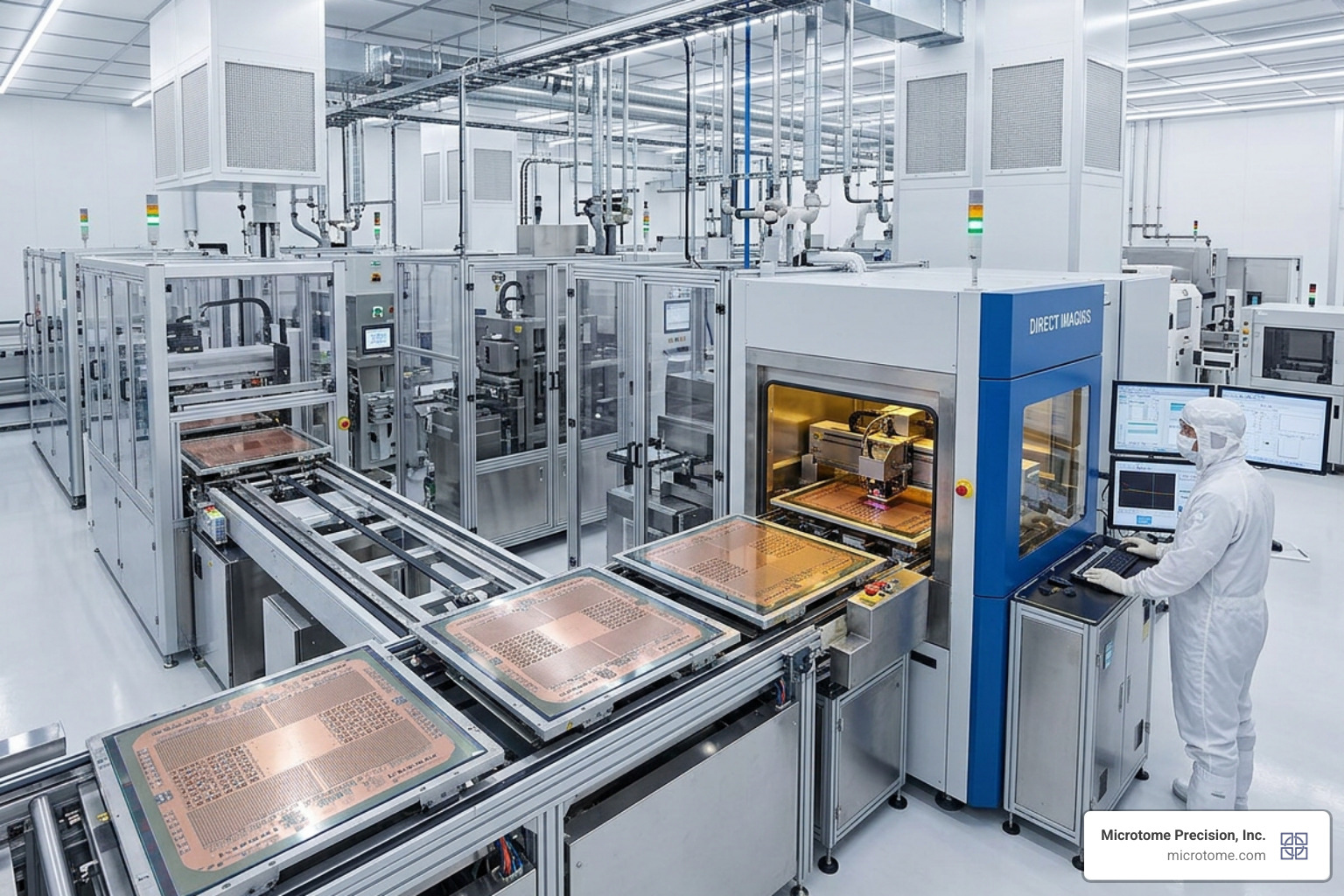
These innovations mean that reticles are being handled more frequently, by a wider variety of robotic end-effectors, and across more diverse cleanroom environments. To support these evolving automated flows, fabs must deploy highly compatible and robust carriers. Our comprehensive line of Reticle Handling Products is engineered to interface seamlessly with advanced robotic grippers and load ports, ensuring secure, contamination-free transfer at every stage of the lithography cell.
Frequently Asked Questions
Why does reticle stitching increase silicon interposer costs?
Reticle stitching dramatically increases costs because it reduces scanner throughput. In standard monolithic exposure, the scanner exposes the entire die in a single shot. With stitching, the scanner must perform multiple exposures per layer (e.g., three exposures for a 3.3X reticle interposer). The wafer stage must step, settle, align, and expose multiple times for every single interposer on the wafer. This added stage overhead slows down the lithography tool, which is already the most expensive machine in the fab. Additionally, any overlay error or defect at the stitching boundary will ruin the entire interposer, compounding yield losses.
How does EMIB-T compare to traditional silicon interposers in wafer utilization?
Traditional silicon interposers require manufacturing a single, massive piece of silicon that spans the entire footprint of the chiplet complex. Because these interposers are large and square, and silicon wafers are round, wafer utilization can drop to as low as 60% near the wafer edges. EMIB-T, on the other hand, uses very small, localized silicon bridges only at the boundaries where chiplets connect. These tiny bridges can be packed tightly across a silicon wafer, achieving approximately 90% wafer utilization. The rest of the large package footprint is made up of cost-effective organic substrate materials.
What is the dominant electrostatic risk to advanced lithography reticles?
The dominant electrostatic risk is Electric Field induced Migration (EFM), which was discovered through Microtome Precision’s pioneering research in 2003. Unlike standard ESD, which requires a physical spark discharge, EFM occurs at very low electrostatic field strengths. External electric fields polarize sub-micron cleanroom particles, pulling them directly onto the reticle surface where they cause printing defects. Furthermore, these fields can cause the chrome patterns on the mask to migrate over time.
Conventional ESD controls, like static-dissipative plastics, do not block these electric fields. Only a complete, all-metal Faraday cage—such as those used in our Reticle Protection Products—can shield the reticle from EFM.
Conclusion
As the semiconductor industry pushes past the physical limits of monolithic silicon to build the next generation of AI and HPC accelerators, advanced reticle packaging will continue to dictate the economics of high-performance computing. Whether your fab relies on stitched silicon interposers, embedded silicon bridges like EMIB, or high-density panel-level packaging, success ultimately depends on two things: sub-micron physical precision and flawless contamination control.
At Microtome Precision, Inc., in Colorado Springs, Colorado, we believe that reticle protection is not just a part of the process—it is our entire business. Since 1989, we have remained the leading independent manufacturer of reticle carriers, offering SEMI E111 and SEMI E112 compliant, all-metal Faraday-cage single reticle pods and multi-reticle cassettes. By shielding your high-value photomasks from the invisible threat of EFM and cleanroom contamination, we help you secure your yield, maximize tool uptime, and successfully scale past the reticle limit.
To learn more about how our all-metal carriers can protect your advanced lithography assets and integrate into your automated fab flows, explore our Compatibility Information or contact our engineering team in Colorado Springs today.