
Everything You Need to Know About Advanced Reticle Carriers

Why Choosing the Right Advanced Reticle Carriers Can Make or Break Your Yield
Advanced reticle carriers are specialized protective enclosures that safeguard photomasks — the master templates used to print circuit patterns onto silicon wafers — during storage, handling, and transport inside semiconductor fabs and mask shops.
Here’s a quick comparison of the main types to match your needs:
| Carrier Type | Best For | Key Protection |
|---|---|---|
| Reticle SMIF Pod (RSP) | 150mm/200mm DUV reticles | Contamination, ESD, UV |
| EUV Reticle Pod | EUV lithography | All-metal, Faraday-cage, vacuum-compatible |
| Multi-reticle Cassette | Batch storage/transport | Contamination control, purge gas |
| All-metal Pod | High-ESD/EFM risk environments | Full Faraday-cage shielding |
Reticles are among the most expensive and fragile components in semiconductor manufacturing. A single advanced EUV reticle can cost over one million dollars and take weeks to qualify. One particle, one electrostatic event, or one contamination exposure can transfer defects to thousands of wafers before anyone notices.
The stakes are high — and getting higher. The global reticle pod market is valued at $0.28 billion in 2026 and is projected to reach $0.56 billion by 2035, driven by the growing complexity of semiconductor devices and the rapid adoption of EUV lithography.
Yet many fabs still rely on carrier solutions that were not designed with the full range of reticle failure modes in mind — particularly EFM (Electric Field induced Migration), a damage mechanism that occurs at far lower electrostatic stress than conventional ESD.
I’m Matt Pilarski, President of Microtome Precision, Inc., the longest-established independent designer and manufacturer of advanced reticle carriers, with research roots going back to 1989 and the discovery and characterization of EFM in 2003. My work includes contributions to SEMI Standards E111, E112, and E163 — the core industry standards governing reticle pod design and compatibility.
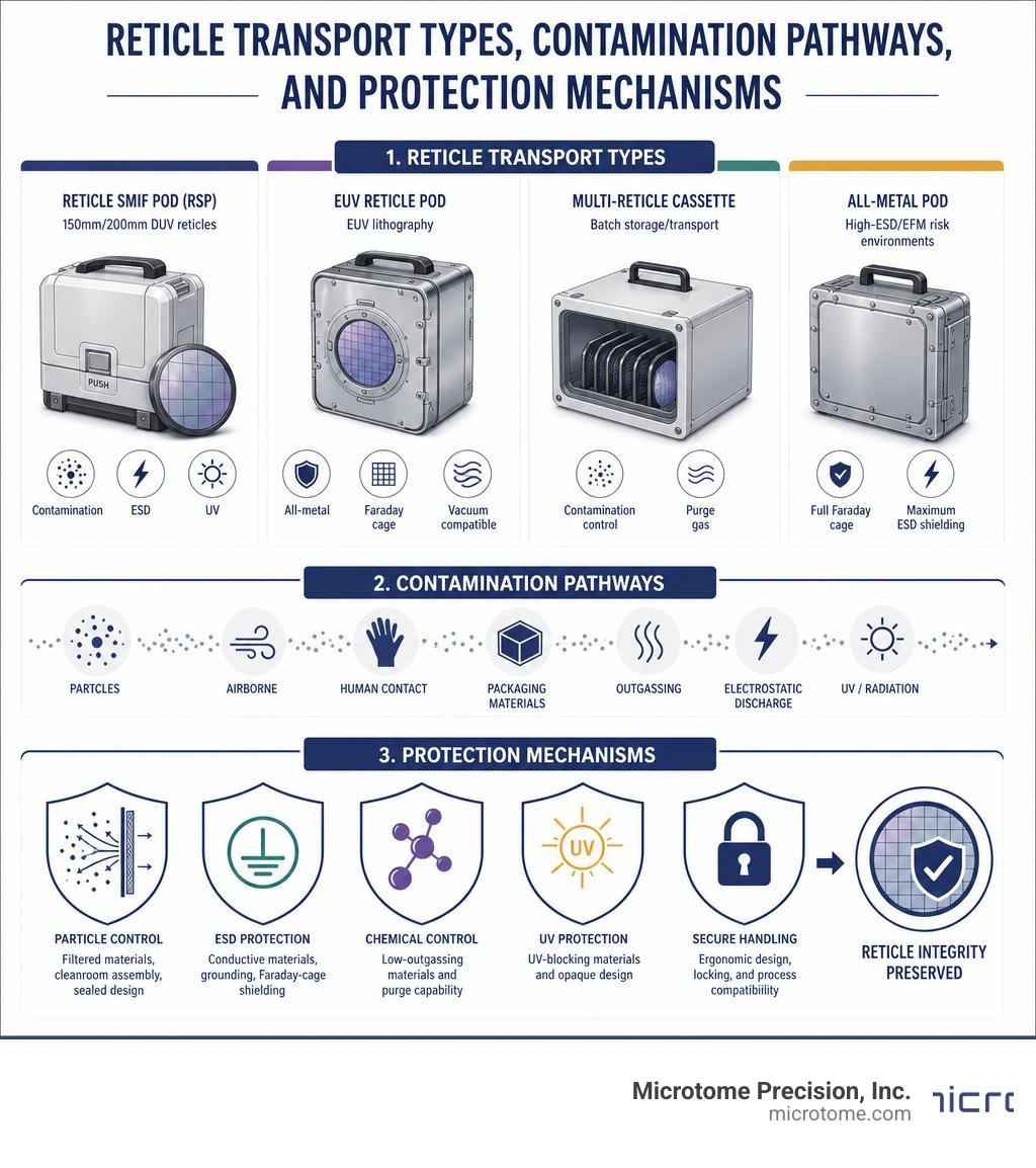
Key Contamination Risks and the Evolution of Advanced Reticle Carriers
To appreciate the design of modern advanced reticle carriers, we first have to look at the invisible battlefield inside the fab. In sub-10nm nodes, even a single particle measuring just a few nanometers can ruin an entire production run. The major threats to a photomask’s survival come from three fronts: particulate contamination, electrostatic damage, and chemical outgassing.
Historically, simple plastic boxes were used to move reticles. However, as circuit geometries shrank, these basic carriers became a major source of yield loss. Plastics naturally build up static charges. When a charged carrier moves through the cleanroom, it generates strong electric fields. These fields act like microscopic tractor beams, pulling airborne molecular contaminants (AMCs) and sub-micron particles straight toward the active surface of the reticle.
Furthermore, traditional plastic carriers suffer from outgassing. Over time, the polymers and plasticizers used in standard carriers release trace chemicals. These gaseous contaminants deposit onto the quartz substrate and chrome patterns, creating “haze” defects when exposed to high-energy lithography light.
To combat this, the industry transitioned toward highly specialized materials and mechanical standards. According to the Reticle POD Market Size, Share & Future Analysis 2035, the demand for high-performance protection is skyrocketing. Fabs are realizing that preventing contamination at the carrier level is far more cost-effective than frequent, high-risk reticle cleaning cycles.
Electrostatic Discharge (ESD) and EFM Shielding in Advanced Reticle Carriers
Electrostatic discharge (ESD) is a well-known villain in semiconductor manufacturing. A sudden, high-voltage spark can instantly melt the fine chrome or molybdenum silicide lines on a photomask. But there is an even sneakier threat: Electric Field induced Migration (EFM).
EFM occurs when a reticle is exposed to strong external electric fields. Even without a direct spark, these fields polarize the metallic structures on the mask, causing metal ions to migrate across the quartz substrate. Over time, this migration distorts the printed circuit lines and causes catastrophic lithography defects.
To prevent both ESD and EFM, we design and manufacture carriers with true Faraday-cage protection. By utilizing an all-metal outer construction, our carriers block external electric fields entirely. Inside the carrier, we also focus on the physics of the electrostatic decay rate, which is governed by the RC (resistance-capacitance) time constant.
When a reticle is loaded into a carrier, any residual charge must be discharged quickly and safely. According to patented electrostatic models, the height of the support pins inside the carrier plays a crucial role:
- A support pin height of 200 microns prevents particles of 147nm radius or larger from being attracted.
- A height of 400 microns prevents particles of 75nm or larger.
- A height of 1000 microns prevents particles of 22nm or larger.
- To achieve optimal performance, a support pin height range of 1150 to 4000 microns balance capacitance reduction with stability, allowing the residual charge to safely decay through grounded contact points.
Our flagship E-Pod Product leverages this precise physics to provide unmatched EFM shielding and rapid charge dissipation, ensuring your reticles remain completely isolated from harmful cleanroom fields.
Mechanical Self-Positioning and Edge-Contact Restraints
Preventing contamination and static is only half the battle; we also have to protect the reticle from physical damage during high-speed robotic transport. If a reticle shifts or slides inside its carrier, the resulting friction can generate thousands of sub-micron particles.
Advanced carriers solve this problem using clever mechanical engineering. The carrier cover is equipped with diagonal-edge self-positioning tabs. As the carrier lid is closed, these tabs gently guide the reticle into perfect alignment, eliminating the need for high-precision manual placement.
Once positioned, the reticle is held in place by resilient arm restraints that contact only the outer edges and corners of the quartz substrate. By avoiding any contact with the active pattern area, we eliminate the risk of pattern scratches or surface degradation. Our commitment to this level of design precision is why we say that Reticle Protection is not just a feature—it is our core business.
Comparing Reticle SMIF Pods (RSP) and EUV Reticle Pods
As lithography technology split into Deep Ultraviolet (DUV) and Extreme Ultraviolet (EUV) pathways, the design of advanced reticle carriers split with it. Understanding the differences between these two carrier classes is essential when planning your fab’s transport and storage strategy.
| Specification / Feature | Reticle SMIF Pod (RSP 150/200) | EUV Reticle Pod |
|---|---|---|
| Primary Lithography | DUV (ArFi, KrF, i-Line) | EUV (13.5nm wavelength) |
| Pellicle Compatibility | Polymer pellicles | Very limited clearance; requires specialized metal/carbon pellicles |
| Base Material | ESD-safe Polymers or Metal | High-purity PEEK or All-Metal (Aluminum/Nickel) |
| Internal Environment | Atmospheric pressure with inert gas purge | Dual-pod design (inner vacuum, outer atmospheric) |
| Shielding Type | Electrostatic dissipative | Full Faraday-cage shielding |
| Standard Compliance | SEMI E100, E111 | SEMI E112, E152 |
Choosing the wrong pod type can lead to immediate compatibility issues with your lithography scanners. For detailed integration specs, you can refer to our Compatibility Information page to ensure a seamless match with your specific lithography tools.
Standard Mechanical Interface (SMIF) Pod Features
The Reticle SMIF Pod (RSP) has been the workhorse of the lithography department for decades. Designed to transport 150mm reticles within a standardized 200mm mechanical interface, these pods isolate the reticle from the cleanroom environment during transport.
Key features of high-performance RSPs include:
- Door Purge Interface: Allows the continuous flow of ultra-pure nitrogen or clean dry air (CDA) through the pod to sweep away moisture and airborne molecular contaminants.
- Info Pads: Provide mechanical keying and identification to prevent the pod from being misaligned or loaded into the wrong tool port.
- UV Blocking Materials: High-quality polymer or coated windows block light at wavelengths ≤470 nm, protecting photosensitive chemically amplified resists or pellicles from accidental exposure.
While plastic RSPs are common, they are prone to polymer outgassing over time. At Microtome Precision, we address this by offering all-metal and hybrid SMIF pods that combine the mechanical interface of the RSP with the low-outgassing, Faraday-shielding properties of metal. Check out our Products Overview to see how we blend these technologies.
EUV Pod Innovations for Next-Generation Lithography
EUV lithography utilizes a 13.5nm light wavelength, which is absorbed by almost all matter—including glass and air. Because of this, EUV scanners must operate under an ultra-high vacuum. This requirement completely changes how the reticle carrier must behave.
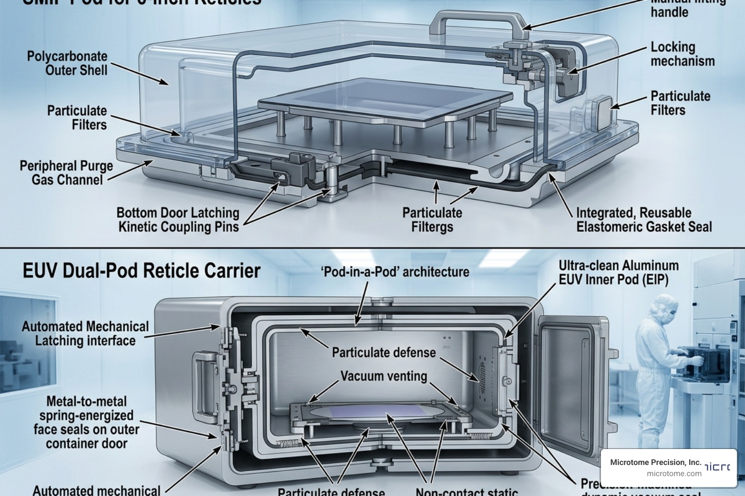
EUV pods use a unique “dual-pod” design:
- Inner Pod (EIP): Holds the reticle securely and is designed to enter the vacuum chamber of the EUV scanner. It must be completely metal-free or made of vacuum-compatible, ultra-low outgassing materials (like specialized ESD PEEK or metal) to prevent vacuum contamination.
- Outer Pod (EOP): Encloses the Inner Pod, protecting it from atmospheric contamination, moisture, and mechanical shocks during transport via automated overhead hoist systems.
Because EUV reticles do not traditionally use a protective pellicle (or use extremely thin, fragile ones), the inner pod must provide absolute particle protection. This requires a true all-metal construction that acts as a robust Faraday-cage, shielding the mask from any electrostatic attraction forces that could pull particles onto the active reflective multilayer coatings.
AMHS Integration and Yield Benefits in High-Volume Manufacturing
In a modern high-volume manufacturing (HVM) fab, humans rarely touch reticle carriers. Automated Material Handling Systems (AMHS) use Overhead Hoist Transport (OHT) robots to fly carriers along tracks suspended from the cleanroom ceiling, delivering them to automated storage stockers and tool load ports.
This automated environment requires extreme dimensional consistency. Advanced reticle carriers feature high-precision OHT flanges that allow robotic grippers to secure the pod with millimeter-level accuracy.
By integrating advanced carriers into your AMHS, you unlock major yield and operational benefits:
- Reduced Defect Density: Minimizing human handling eliminates the primary source of random particle contamination.
- Optimized Purge Consumption: Modern carriers feature high-conductance purge valves that achieve rapid gas replacement with minimal nitrogen consumption, lowering utility costs.
- Asset Life Extension: Secure edge-contact restraints and vibration-damping materials protect delicate phase-shift masks and EUV reticles from mechanical stress, extending their operational lifespan.
- Lower Total Cost of Ownership (TCO): Preventing a single reticle damage event can save hundreds of thousands of dollars in replacement costs and prevent hours of unplanned scanner downtime.
Whether you are an Integrated Device Manufacturer (IDM) producing high-volume memory or a foundry running hundreds of custom ASIC designs, advanced carriers keep your lithography bays running at peak throughput.
Industry Standards and Compliance for Advanced Reticle Carriers
To ensure that a reticle carrier will work seamlessly across different scanner brands, stockers, and AMHS systems, it must adhere strictly to international SEMI standards:
- SEMI E100: Defines the physical dimensions and interface specifications for 200mm reticle SMIF pods.
- SEMI E111: Establishes the mechanical and environmental requirements for reticle carriers used in automated fabs.
- SEMI E112: Specifies the standards for EUV reticle pods and their interfaces with exposure tools.
At Microtome Precision, our designs meet and exceed these standards. We also understand that even the best carriers wear out over time. That is why we offer comprehensive Support and Repair services to inspect, clean, and recalibrate your carrier fleet, ensuring ongoing compliance and peak ESD performance.
All-Metal Cassettes for Reticle Storage and Process Integration
For long-term storage and bare reticle shipping between mask shops and fabs, multi-reticle cassettes are often preferred. These cassettes allow multiple photomasks to be stored in a highly compact footprint.
By utilizing all-metal construction for our cassettes, we provide a clean, robust, and highly durable storage environment. Metal cassettes do not degrade under UV light, do not outgas organic compounds, and offer built-in electrostatic grounding when placed on storage shelves. This ensures that whether your reticles are active on the scanner floor or resting in a stocker, they remain in a pristine, particle-free state.
Frequently Asked Questions About Advanced Reticle Carriers
What is the difference between EUV and non-EUV reticle pods?
EUV reticle pods use a dual-pod design (an inner vacuum-compatible pod and an outer protective pod) to interface with the vacuum chambers of EUV scanners. Non-EUV pods (like standard RSPs) are single-pod designs used in atmospheric DUV lithography systems. EUV pods require much stricter outgassing controls and absolute Faraday-cage shielding because EUV reticles are highly sensitive to particle defects.
How do advanced reticle carriers prevent electrostatic damage?
They utilize highly conductive or dissipative materials (such as metals or ESD-safe polymers) to ground any electrical charges. By forming a complete Faraday-cage around the reticle, they block external electric fields from penetrating the carrier. Additionally, optimized support pin heights reduce capacitance, allowing any residual charge on the reticle to dissipate safely and quickly.
Why are SEMI standards important for reticle transport?
SEMI standards (like E100 and E111) define the exact dimensions, latch locations, and robotic interface points of the carriers. Without these standards, it would be impossible for automated transport systems (AMHS) and lithography scanners from different manufacturers to safely lift, open, and process the carriers.
Conclusion
In advanced semiconductor manufacturing, your yield is only as good as your contamination control. As feature sizes continue to shrink, relying on legacy plastic carriers is a risk your balance sheet cannot afford.
At Microtome Precision, Inc., we have spent decades perfecting the art and science of reticle protection. Based in Colorado Springs, Colorado, we design and manufacture all-metal reticle carriers and SMIF pods that offer true Faraday-cage protection against EFM and particulate contamination. Our solutions are built on proprietary research and SEMI standards that we have helped develop since 1989.
Protect your investments, secure your yield, and keep your lithography tools running at maximum capacity. Explore our complete line of advanced transport solutions on our Products Overview page, or contact our engineering team today to discuss your custom fab integration needs.