
In-Depth Guide to SEMI Standard SMIF
What Is the SEMI Standard SMIF — and Why Does It Matter?
The SEMI standard SMIF (Standard Mechanical Interface) is a set of specifications that defines how sealed pods transport and protect wafers and reticles from contamination during semiconductor manufacturing.
Here’s a quick summary of the key facts:
| Topic | Key Detail |
|---|---|
| What SMIF stands for | Standard Mechanical Interface |
| Governing standard | SEMI E19 (originally published 1991) |
| Wafer sizes covered | 100 mm, 125 mm, 150 mm, and 200 mm |
| How it works | Sealed pod mates with equipment door; wafers never exposed to ambient air |
| Key benefit | Up to 100x cleaner than open cassette transfers in ISO class-5 environments |
| 300 mm equivalent | FOUP (Front Opening Unified Pod) |
| Also used for | Reticles and photomasks (SEMI E100, SEMI E111) |
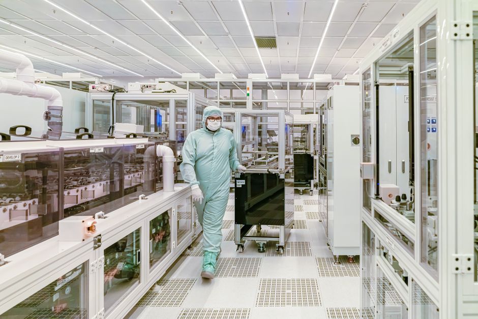
Even in a modern cleanroom, the air is not particle-free. Cleanrooms are classified by particle count per cubic meter — but particles still exist. And in semiconductor manufacturing, even a single microscopic particle landing on a wafer or reticle can destroy multiple chips or ruin a photomask that took weeks to qualify and cost over a million dollars.
SMIF was developed in the 1980s to solve exactly this problem. The core idea is simple: enclose wafers in a sealed pod, and only open that pod inside a filtered, controlled mini-environment built into the processing equipment. No exposure to open cleanroom air. No contamination from manual handling. No turbulence from room airflow.
The system was pioneered by a team at Hewlett-Packard — sometimes called the “micronauts” — and eventually became a formal SEMI standard that fabs worldwide have built their material handling systems around. Over 200 facilities for 200 mm wafers alone have been constructed using SMIF technology since the early 1990s.
I’m Matt Pilarski, President of Microtome Precision, Inc., where we’ve specialized in reticle carrier design and SEMI standard SMIF compliance since 1989 — including developing the first E111-compliant single reticle pod approved by all major lithography companies. In this guide, I’ll walk you through how the standard works, what the different specifications cover, and what it means for protecting high-value reticles in your fab.
Understanding the SEMI Standard SMIF Specifications
At its heart, the SEMI standard SMIF is all about creating a standardized mechanical interface. When you are running a fab, you use equipment from dozens of different vendors—lithography systems, metrology tools, etch systems, and deposition chambers. For automation to work, every single one of these tools must interact with your wafer carriers in the exact same way.

This is where the SEMI E19 Standard Specification comes into play. Originally published in 1991 and technically approved by the Physical Interfaces & Carriers Global Technical Committee, SEMI E19 defines the mechanical dimensions, tolerances, and operational steps required for standard mechanical interfaces.
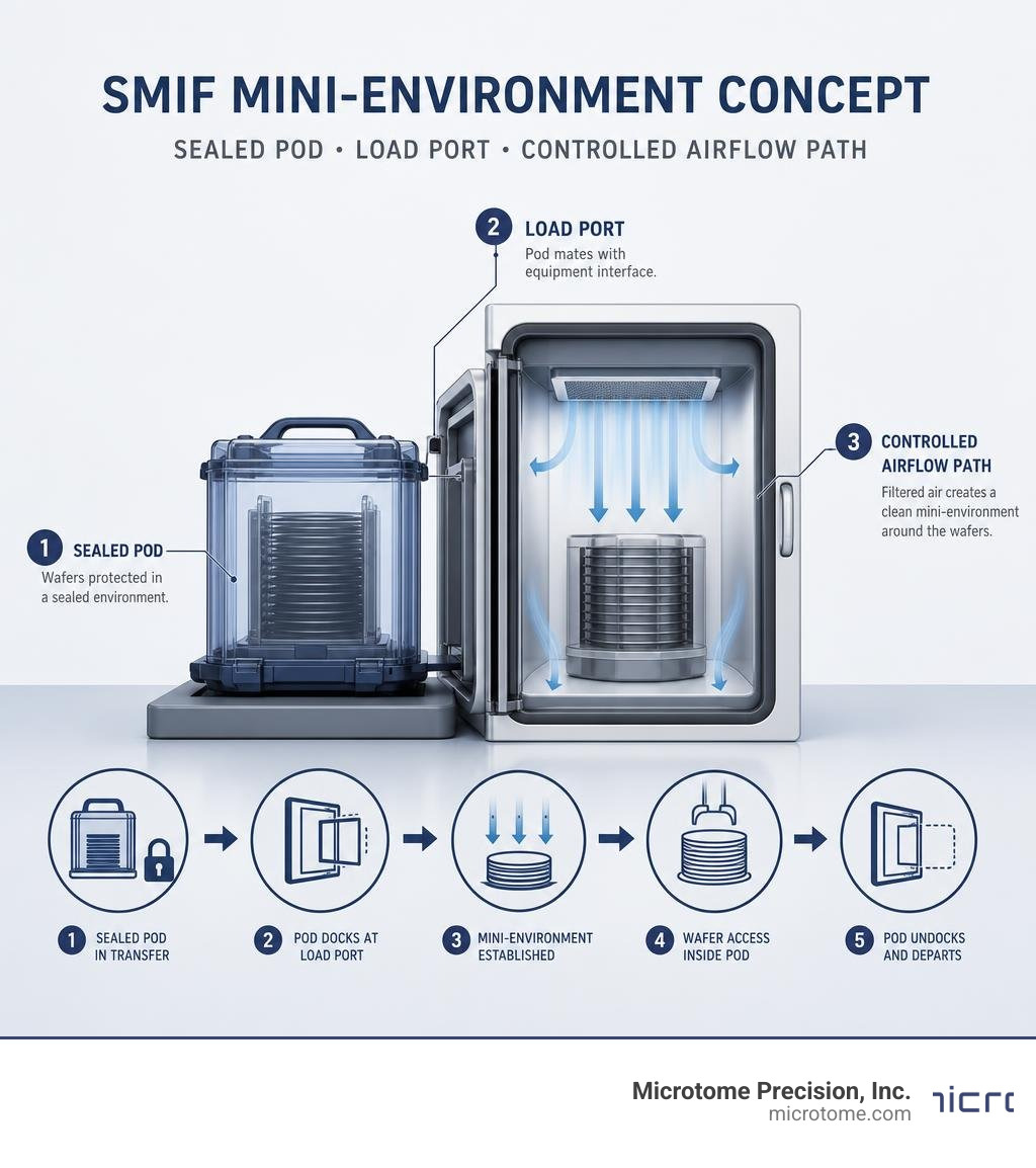
The standard ensures that when a cassette container (the SMIF pod) is placed onto a processing tool’s load port, the physical interface is completely seamless. The system concept relies on a highly coordinated mechanical sequence:
- The SMIF pod, containing a cassette of wafers, is loaded onto the port.
- The door of the pod mates perfectly with the door of the equipment’s load port.
- The two doors lock together, trapping any surface contamination between them.
- The combined door assembly lowers or retracts into the equipment canopy (the mini-environment).
- The wafer cassette is transferred into the tool’s ultra-clean processing area without ever seeing the ambient cleanroom air.
By strictly limiting the scope of SEMI E19 to physical interfaces, the standard allows manufacturers to innovate on the materials and internal designs of the pods while ensuring absolute mechanical compatibility across the industry.
The Evolution of SEMI Standard SMIF and Subordinate Standards
As wafer sizes grew and automation became more sophisticated, the original SEMI E19 standard needed to evolve. To maintain clarity, SEMI structured E19 with several subordinate standards, while other branches of the standard were eventually published separately or withdrawn.
Here is how the family of standards is broken down:
- SEMI E19.1, E19.2, and E19.3: These subordinate standards define the precise specifications for the 100 mm (4-inch), 125 mm (5-inch), and 150 mm (6-inch) versions of the SMIF port. They outline the exact physical dimensions required to establish a reliable base for port standardization.
- SEMI E19.4: This standard specifies the interface for 200 mm SMIF systems. Because 200 mm wafers became the workhorse of the industry throughout the 1990s and 2000s, E19.4 is one of the most widely implemented standards in legacy and specialty fabs today.
- SEMI E19.5: This was the specification drafted for a 300 mm Bottom-Opening SMIF system. However, as the industry transitioned from 200 mm to 300 mm wafers, the mechanical dynamics changed. Wafers became heavier and more prone to sag, making bottom-opening mechanical interfaces highly complex and risky. Consequently, SEMI E19.5 was withdrawn as the industry moved toward front-opening designs.
For fabs running mature nodes, understanding these legacy standards is critical for maintaining tool compatibility. At Microtome Precision, we closely monitor these specifications to ensure our custom engineering projects align perfectly with your existing toolsets. You can learn more about how we handle these specifications on our Compatibility Information page.
Key Components of a SEMI Standard SMIF System
To understand how a SEMI standard SMIF system operates, it helps to break down the physical hardware into its core components:
- The SMIF Pod: This is the portable, sealed enclosure used to transport the wafer cassette. It consists of a protective box (the shell) and a bottom-opening door. The pod is designed to maintain a highly controlled internal environment with low-outgassing materials and excellent airtightness.
- The Bottom-Opening Door: Unlike a standard container lid, the SMIF pod door is located at the bottom. It features precise latching mechanisms that only release when securely mated to a compatible load port.
- The Load Port / Port Assembly: This is the physical interface mounted on the processing equipment. It contains the registration pins, latch activators, and the elevator mechanism that lowers the mated doors into the tool.
- The Equipment Canopy (Mini-environment): This is the enclosed volume inside the processing tool. It is equipped with dedicated Fan Filter Units (FFUs) using Ultra-Low Penetration Air (ULPA) filters to maintain an ISO Class-1 or Class-2 environment directly around the wafers.
By isolating the wafers inside this small, highly controlled envelope, fabs can avoid the massive energy costs of maintaining an entire cleanroom ballroom at extremely strict cleanliness levels.
How SMIF Technology Protects Wafers and Reticles
The primary goal of any SMIF system is contamination control. By restricting the open handling of wafers to highly localized “mini-environments,” SMIF technology dramatically reduces particle deposition.

When a SMIF pod is docked, the air inside the interface is carefully managed. Many modern SMIF ports incorporate active purging systems. These systems introduce ultra-pure nitrogen ($N_2$) or Extreme Clean Dry Air (XCDA) into the pod through dedicated purge valves. This purging process displaces ambient moisture, oxygen, and airborne molecular contaminants (AMCs), which are known to cause wafer degradation, crystal growth, or reticle haze.
Furthermore, electrostatic discharge (ESD) is a severe threat in semiconductor manufacturing. Static charges attract particles like a magnet and can physically destroy sensitive microelectronic structures. To combat this, compliant SMIF pods utilize static-dissipative materials and conductive path structures at the wafer and carrier contact areas. This allows any static buildup to safely discharge to the ground through the load port interface.
At Microtome Precision, we take this protection a step further. While standard plastic pods offer basic ESD protection, our specialty is designing and manufacturing all-metal pods. These metal enclosures act as a true Faraday cage, providing complete mitigation against Electrostatic Fields (EFM) and preventing RF interference from disrupting sensitive reticles or wafers. You can explore our full range of high-protection carriers on our Products Overview page.
Contamination Control and Cleanliness Statistics
The impact of SMIF technology on fab yields is backed by clear, historical research data. According to SEMI research, SMIF systems provide vastly superior wafer protection compared to traditional open cassette transfers:
- 100x better cleanliness when operating in an ISO Class-5 facility.
- 30x better cleanliness when operating in an ISO Class-4 facility.
- 10x better cleanliness when operating in an ISO Class-3 facility.
Essentially, SMIF decouples the cleanliness of the wafer from the cleanliness of the ambient cleanroom. This means a fab can achieve ISO Class-1 or Class-2 wafer protection inside the mini-environment while operating the surrounding cleanroom ballroom at a much less expensive ISO Class-5 or Class-6 standard. This shift has saved the semiconductor industry billions of dollars in cleanroom construction and operational energy costs over the past three decades.
For detailed technical discussions on how these micro-environments manage particle counts and airflow, you can refer to the SMIF FAQ and Technical Support resources.
Reticle Protection and the SEMI E100 Standard
Wafers are not the only high-value assets in a fab that require SMIF-level protection. Photomasks (or reticles) are the master templates used in photolithography. Because any dust particle on a reticle will be projected and printed onto every single wafer on the line, protecting reticles is of paramount importance.
The industry standard governing reticle SMIF pods (RSPs) is the SEMI E100 Specification. This standard specifies the physical interfaces and dimensions for pods used to transport and store 6-inch (152 mm) or 230 mm reticles.
Key technical aspects of the SEMI E100 standard include:
- Physical Interfaces Only: To encourage design innovation, the standard purposefully avoids specifying material requirements or micro-contamination limits, focusing instead on physical interchangeability.
- Pellicle Exclusion Volumes: Reticles use a thin, protective film called a pellicle to keep dust away from the chrome image plane. The E100 standard defines strict exclusion volumes (e.g., a width limit of 129 mm for 6-inch reticles and 151 mm for 230 mm reticles) to ensure that automated end-effectors and tool interfaces never touch or damage the delicate pellicle.
- Kinematic Coupling: RSPs utilize highly precise kinematic coupling pins on the bottom door to ensure sub-millimeter placement accuracy when docking with lithography tools.
A classic example of an E100-compliant carrier is the RSP150 reticle SMIF pod. Designed to hold a single 152 mm x 152 mm x 6.35 mm reticle, the RSP150 weighs approximately 760 grams empty and 1100 grams when loaded with a reticle. These pods often incorporate 0.1-micron breather filters to allow pressure equalization during transport without introducing outside particles.
Comparing SMIF and FOUP Technologies
As semiconductor technology progressed to larger wafer sizes, the physical mechanisms used to transport them had to change. This led to the development of the Front Opening Unified Pod (FOUP).
Here is a direct comparison of how these two standard carrier technologies stack up:
| Feature | SMIF (Standard Mechanical Interface) | FOUP (Front Opening Unified Pod) |
|---|---|---|
| Primary Wafer Sizes | 100 mm, 125 mm, 150 mm, 200 mm | 300 mm, 450 mm |
| Door Orientation | Bottom-opening | Front-opening |
| SEMI Standards | SEMI E19, E19.4, E100, E111 | SEMI E47.1 |
| Mechanical Action | Pod door lowers vertically into the tool | Pod door opens horizontally forward |
| Automation Focus | Often manual or bottom-loading AGVs | Overhead Hoist Transport (OHT), fully automated |
| Weight Profile | Lighter, optimized for smaller payloads | Heavier, designed for 25-wafer 300mm payloads |
While SMIF is the undisputed standard for 200 mm and smaller wafer lines, FOUP is the universal standard for 300 mm manufacturing. If you are operating a bridge tool or transitioning a line, choosing the right carrier configuration is critical. You can view our specialized solutions for these environments, such as our high-durability E-Pod Product, to see how we bridge these technical requirements.
Automation Integration in Modern Fabs
In modern, highly automated fabs, SMIF pods are integrated directly with Material Control Systems (MCS) and Manufacturing Execution Systems (MES). This integration relies on several standardized technologies:
- Overhead Hoist Transport (OHT) and AGVs: Automated Guided Vehicles (AGVs) and overhead rails transport SMIF pods across the fab. The pods are equipped with standardized top-handling flanges and side collar flanges to allow robotic grippers to safely secure them.
- SECS/GEM Communication: Tools communicate with the fab’s host computer using SECS/GEM protocols. When a SMIF pod is loaded, the tool reads the carrier ID and reports the status back to the MES.
- Info Pads: Located on the bottom of the SMIF pod door, these info pads act as physical binary configuration identifiers. By sensing whether specific pins on the load port are depressed by the info pads, the tool instantly knows the carrier’s configuration (e.g., whether it contains a 6-inch reticle or a 230 mm reticle) before starting the mechanical transfer.
Frequently Asked Questions about SEMI SMIF
Why was SMIF technology not feasible for 300mm wafers?
When the semiconductor industry transitioned to 300 mm wafers in the late 1990s and early 2000s, engineering teams quickly realized that bottom-opening SMIF designs were mechanically unfeasible.
A 300 mm silicon wafer is significantly heavier and more flexible than a 200 mm wafer. If you attempt to support a 300 mm wafer cassette from the bottom and lower it vertically, the mechanical stress and gravity cause the wafers to sag. This deflection increases the risk of wafers slipping, chipping, or rubbing against the cassette teeth, generating severe particle contamination.
Furthermore, the elevator mechanisms required to lift and lower a heavy 25-wafer 300 mm cassette vertically would have made the load ports massive and mechanically complex. The front-opening design of the FOUP solved this by keeping the cassette horizontal and sliding the wafers out laterally, minimizing gravitational stress.
What is the difference between SEMI E19 and SEMI E111?
While both standards deal with mini-environments and mechanical interfaces, they target completely different payloads:
- SEMI E19 is the foundational standard for wafer cassettes. It specifies the physical interface parameters for transferring wafer cassettes (100 mm to 200 mm) from a pod into a processing tool.
- SEMI E111 is the specification designed specifically for reticle protection within the lithography bay. It governs single-reticle SMIF pods (like the RSP150) to ensure exact mechanical compatibility with exposure tools (steppers and scanners).
Because reticles are incredibly sensitive to electrostatic fields and chemical outgassing, E111-compliant pods require much tighter material controls and specialized purging capabilities compared to standard E19 wafer pods.
How does a SMIF pod maintain ESD protection?
ESD protection in a SMIF pod is achieved through a continuous conductive path. The shell and door of the pod are molded from engineering plastics embedded with carbon fibers or carbon nanotubes (such as proprietary static-dissipative polymers).
When the wafers or reticles rest inside the carrier, they make contact with conductive support pads. These pads connect to conductive paths running through the pod door to external grounding contact points. When the pod docks with the load port, these contacts align with grounded pins on the tool, safely bleeding off any accumulated static charge before the pod door is unlocked.
Conclusion
The SEMI standard SMIF remains a cornerstone of contamination control and automated material handling in 200 mm wafer fabs and lithography bays worldwide. By isolating high-value wafers and reticles within highly controlled mini-environments, SMIF technology has enabled the industry to push the boundaries of microelectronics while keeping operational costs manageable.
At Microtome Precision, Inc., based in Colorado Springs, Colorado, USA, we have spent nearly four decades perfecting the art of carrier design. Our unique, all-metal pods provide an unmatched level of protection. By acting as a Faraday cage, our carriers mitigate the risks of Electrostatic Fields (EFM) and prevent electromagnetic interference from compromising your critical lithography reticles.
Whether you need a custom-engineered solution to fit a legacy tool, or you require expert maintenance on your existing fleet, our team is here to help. Explore our Support and Repair services to see how we keep your fab running at peak performance.