
Electrostatic Discharge Meaning: Terms Demystified

What Electrostatic Discharge Meaning Really Tells Us — And What It Misses
Understanding the electrostatic discharge meaning is straightforward at first glance:
Electrostatic discharge (ESD) is the sudden, rapid transfer of electric charge between two objects at different electrical potentials — through direct contact, an arc, or dielectric breakdown.
Here is a quick-reference summary:
| Term | Plain-language meaning |
|---|---|
| Electrostatic charge | A buildup of electrical charge on a surface |
| Discharge | The sudden release of that stored charge |
| ESD event | The moment charge jumps between two objects |
| Damage threshold | Some components fail at as little as 30 V |
| Typical human perception | You feel a shock only above ~2,000–4,000 V |
The tricky part? ESD is only part of the electrostatic hazard picture — especially in semiconductor lithography.
Walking across a carpet can generate up to 35,000 volts at low humidity. Yet most people feel nothing until thousands of volts have already built up. For general electronics, standard ESD controls — grounding, dissipative mats, wrist straps — do a reasonable job.
But for photomasks (reticles), the situation is fundamentally different. A reticle can cost over a million dollars and take weeks to qualify. The electrostatic threat that matters most for reticles is not a dramatic discharge event. It is a far subtler mechanism called EFM (Electric Field induced Migration) — and it operates at stress levels far below what conventional ESD protection is designed to stop.
That distinction is what this guide is built around.
I’m Matt Pilarski, President of Microtome Precision, Inc., where we have specialized in reticle carrier design and the electrostatic discharge meaning as it applies to photomask protection since 1989. Microtome’s research team characterized EFM in 2003, identifying a reticle failure mode that standard ESD frameworks simply do not address — and everything we build is designed around closing that gap.
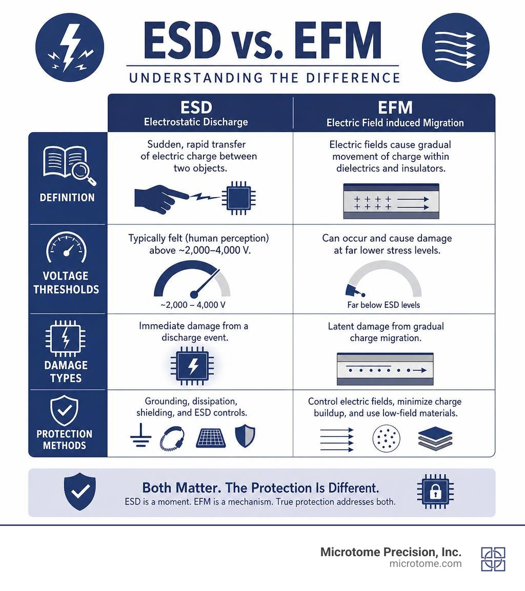
Easy electrostatic discharge meaning word list:
The Technical Electrostatic Discharge Meaning in Semiconductor Environments
To understand how electrostatic hazards compromise a cleanroom, we must look at the formal physics definition. According to the International Electrotechnical Commission (IEC), an electrostatic discharge is the transfer of electric charge between bodies of different electrostatic potentials when they are brought close together or when the dielectric between them breaks down.
In a standard fab, this means a sudden, high-speed flow of current. When two materials with different potentials approach one another, the electric field between them intensifies. If this field strength exceeds the dielectric strength of the surrounding medium (which is approximately 4 to 30 kV/cm for dry air), the air ionizes. This creates a highly conductive plasma path—often visible as a spark—allowing rapid charge equalization.
However, in advanced semiconductor manufacturing, focusing only on visible sparks is a dangerous mistake. Many discharges occur well below the human threshold of perception (typically 2,000 to 4,000 volts). A technician can touch a carrier, cause a 100-volt discharge, and remain completely unaware of the event. Yet, that faint discharge is more than enough to destroy sub-micron structures.
To fully grasp how these events are quantified and managed in the fab, engineers must familiarize themselves with standard verification procedures, which we discuss in detail in An Essential Guide to ESD Test Basics.
Mechanisms of Static Charge Generation and ESD Events
Before an ESD event can occur, an electrostatic charge must first accumulate. In any manufacturing environment, static charge is generated constantly through everyday operations. Understanding how these charges accumulate is the first step toward controlling them.
Tribocharging and Electrostatic Induction
The most common mechanism of charge generation is triboelectric charging (or tribocharging). As defined in EOS/ESD Fundamentals Part 1 | EOS/ESD Association, Inc., tribocharging is the creation of electrostatic charge by the contact and separation of materials.
When two materials are pressed together, their surface atoms interact, and electrons migrate from one material to the other based on their position in the triboelectric series. When they are quickly separated, one material retains a net positive charge (having lost electrons), while the other gains a net negative charge.

Common cleanroom examples of tribocharging include:
- A reticle sliding slightly within a plastic cassette during transport.
- Ultra-pure DI water or low-conductivity solvents flowing through fluoropolymer tubing.
- A technician walking across a cleanroom floor, generating thousands of volts on their body.
The second major mechanism is electrostatic induction. This occurs when a pre-existing charged object is brought near an ungrounded conductor. The electric field from the charged object forces the mobile electrons in the conductor to redistribute, creating highly charged regions of opposite polarity on the conductor’s surface—even though its net charge remains zero. If that conductor then contacts a ground or another object, a sudden discharge occurs. This induction effect is why simply keeping “non-grounded” tools near sensitive areas is highly hazardous.
Standard ESD Testing Models and Susceptibility
To evaluate how sensitive electronic components and photomasks are to these charges, the industry relies on standardized test models. These models simulate real-world discharge paths to establish a device’s withstand voltage:
- Human Body Model (HBM): This model simulates a charged human touching a sensitive device. It is typically represented by discharging a 100 pF capacitor through a 1,500-ohm resistor into the device under test.
- Charged Device Model (CDM): This simulates a situation where the device itself accumulates a charge (e.g., from sliding down a packaging chute) and then discharges when it contacts a metal tool or grounded surface. CDM represents the majority of ESD events in automated assembly lines.
- Machine Model (MM): This model simulates a direct discharge from a charged metal tool or machine part with zero resistance in series.
For a deeper dive into how these models are applied in practice, read The Ultimate Guide to ESD Safe Products.
Why Standard ESD Protection Fails for Photomasks: The Threat of EFM
In general electronics manufacturing, ESD damage usually manifests as physical destruction: oxide rupture, junction filamentation, or metal lines melting. These are often categorized as either catastrophic failures (the device fails immediately) or latent defects (the device is weakened and fails prematurely in the field).
For photomasks (reticles), however, the threat profile is entirely different. Standard ESD protection practices, such as wearing grounded wrist straps or using static-dissipative plastic carriers, are designed to prevent sudden discharges. But they do absolutely nothing to protect against a far more insidious phenomenon: Electric Field induced Migration (EFM).
The Electrostatic Discharge Meaning vs. Electric Field Induced Migration (EFM)
While the electrostatic discharge meaning focuses on the flow of current during a discharge, EFM is driven entirely by the presence of an electric field.
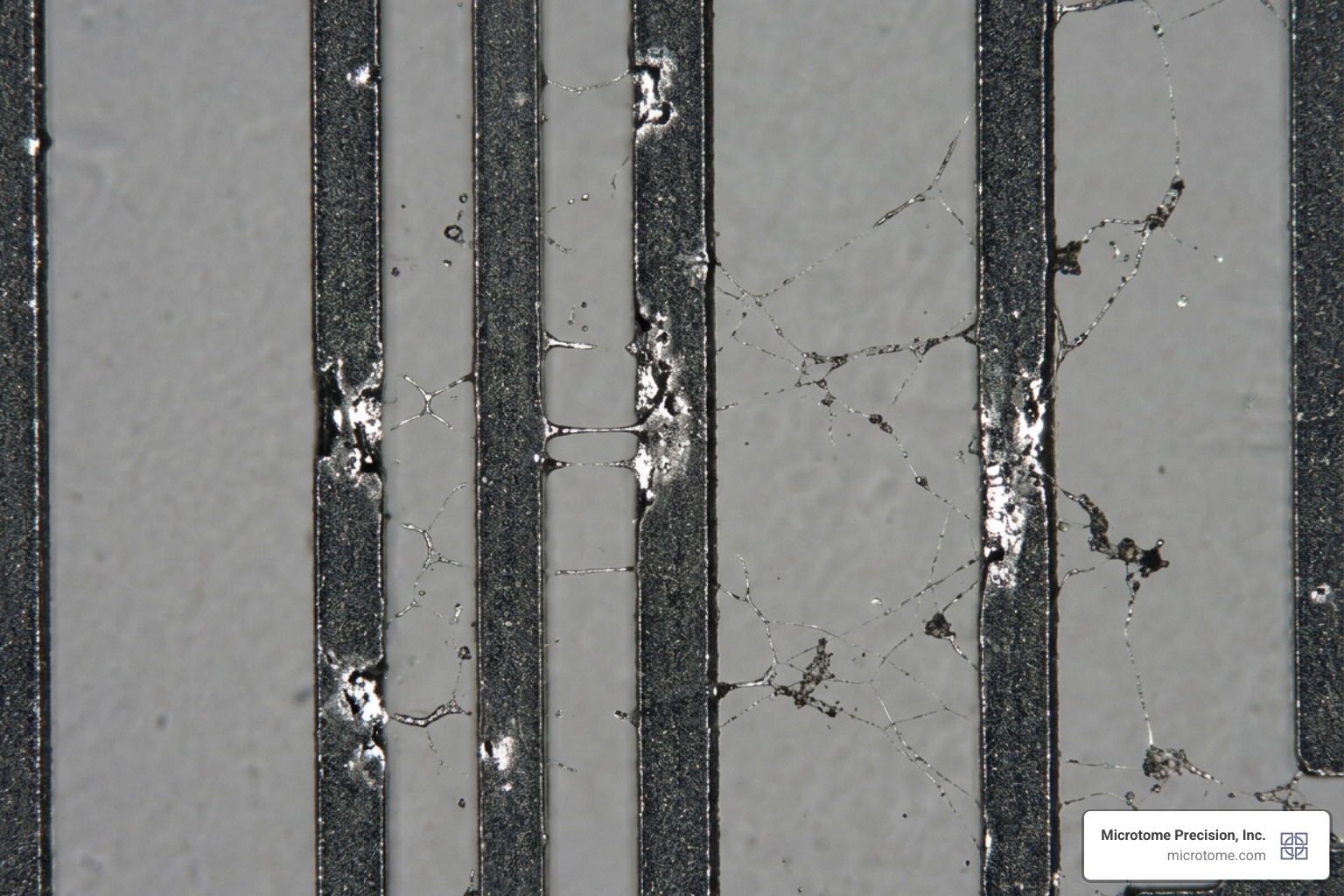
First characterized by our research team at Microtome Precision in 2003, EFM occurs when a photomask is exposed to a localized electrostatic field. Reticles consist of sub-micron chrome features deposited on a non-conductive quartz substrate. When an external electric field penetrates the carrier, it induces a massive potential gradient across these tiny chrome lines.
Because the chrome lines are incredibly narrow and separated by microscopic gaps, even a relatively low external voltage can create an electric field strength of several million volts per meter between adjacent chrome structures. Under this intense electrostatic field stress, chrome atoms physically migrate across the quartz gaps. This migration causes:
- Progressive degradation of the sub-micron chrome lines.
- The formation of microscopic chrome “bridges” or filaments between lines.
- Severe lithographic printing defects, destroying wafer yield long before any physical “spark” or ESD event ever occurs.
The Limitations of Dissipative Plastics and Ionizers
Many fabs mistakenly believe that using static-dissipative or “conductive” plastic SMIF pods and cassettes provides adequate protection for reticles. This is a dangerous misconception.
Static-dissipative polymers are designed to slowly bleed off static charges to ground. However, they are still plastics. They do not block electric fields. When a charged object (like a technician’s sleeve or a plastic tool) comes near a dissipative plastic carrier, the external electric field passes directly through the plastic wall and reaches the reticle inside, inducing EFM.
Furthermore, these engineered plastics often rely on additives that can outgas over time in the cleanroom environment. This outgassing leads to molecular contamination on the reticle surface, resulting in progressive “haze” defects when exposed to high-energy lithography light sources.
| Feature | Static-Dissipative Plastics | All-Metal Faraday Cages |
|---|---|---|
| ESD Prevention | Prevents rapid discharge only | Prevents rapid discharge |
| Electric Field Shielding | Poor (fields pass straight through) | Absolute (100% attenuation) |
| Outgassing Risk | High (additives cause reticle haze) | Zero (pure, cleanroom-grade metals) |
| Durability | Degrades over time and washes | Indefinite life, fully recertifiable |
To learn more about preventing these issues, consider utilizing our specialized Electrostatic Protection Consultancy Service.
Implementing True Electrostatic Shielding in Lithography Fabs
To protect costly photomasks from both ESD and EFM, fabs must move beyond basic grounding and implement true electrostatic shielding.
Faraday Cage Principles for Reticle Protection
A Faraday cage is an enclosure formed by conductive material. When an external electric field encounters a highly conductive metal surface, the free electrons within the metal rapidly redistribute. This charge redistribution creates an internal electric field that is equal and opposite to the external field, completely canceling it out. As a result, the net electric field inside the enclosure is exactly zero.
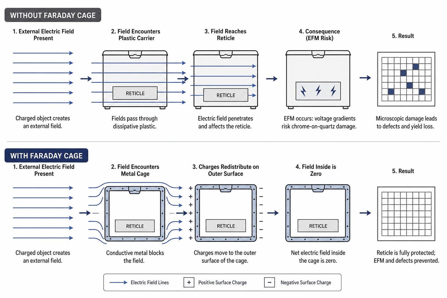
By housing a reticle inside an all-metal, highly conductive enclosure, you ensure that external electric fields—regardless of their strength—cannot penetrate the carrier. This eliminates the voltage gradients across the chrome-on-quartz features, preventing EFM entirely.
This shielding principle is recognized by international standards bodies. To ensure maximum yield protection, reticle carriers should comply with SEMI standards, specifically SEMI E111 (specifications for single reticle SMIF pods) and SEMI E112 (specifications for multi-reticle cassettes).
The Role of All-Metal Carriers in Preventing EFM and ESD
At Microtome Precision, Inc., we design and manufacture all-metal reticle carriers (cassettes and SMIF pods) engineered specifically to act as robust Faraday cages.
Constructed from precision-machined, cleanroom-grade aluminum, our carriers provide absolute electric field shielding. Because they are entirely metallic, they do not outgas, eliminating the risk of chemical contamination and haze on your photomasks. They are designed to integrate seamlessly with both modern and legacy lithography tools, maintaining strict compliance with SEMI standards.
To keep your fleet of carriers performing at their peak, we also offer a comprehensive cleanroom-based recertification program. Learn more about our maintenance options by visiting our Support and Repair page, or explore our full lineup of Products.
Frequently Asked Questions about Electrostatic Discharge Meaning
What is the exact electrostatic discharge meaning in cleanrooms?
In a semiconductor cleanroom, the electrostatic discharge meaning refers to the rapid, uncontrolled transfer of static charge between tools, operators, and silicon wafers or photomasks. Because cleanroom air is kept at a strictly controlled relative humidity (typically 30% to 50% to prevent condensation and microbial growth), static charges generate easily and dissipate slowly. ESD in the cleanroom not only destroys sensitive microstructures directly but also causes Electrostatic Attraction (ESA), pulling airborne particles onto wafers and reticles, which leads to severe imaging defects.
How does EFM differ from standard ESD?
Standard ESD requires a physical discharge path—a spark or current flow—to cause damage. EFM (Electric Field induced Migration) requires no physical contact or discharge. It is caused purely by the stress of an external electrostatic field penetrating a carrier. This field forces the chrome atoms on a reticle to migrate across the quartz substrate, degrading sub-micron lines at voltage levels far below the threshold of standard ESD events.
Why are static-dissipative plastics risky for reticles?
Static-dissipative plastics are excellent for general-purpose ESD workbenches, but they are inadequate for reticle protection. They do not block electric fields, allowing EFM-inducing fields to pass directly through to the photomask. Additionally, the chemical additives used to make these plastics dissipative can outgas in the fab, depositing carbon-based contaminants on the reticle that cook under lithography lasers, creating progressive reticle haze.
Conclusion
Demystifying the electrostatic discharge meaning reveals that managing electrostatic hazards in a semiconductor fab requires looking far beyond simple sparks. While standard ESD protection is sufficient for general electronics, photomasks demand a fundamentally different approach. The threat of Electric Field induced Migration (EFM) means that static-dissipative plastics and air ionizers are simply not enough—and can often introduce new contamination risks.
Protecting your lithography yield requires absolute electrostatic shielding. Since 1989, Microtome Precision, Inc. has been the independent leader in reticle protection. Our all-metal, SEMI-compliant SMIF pods and cassettes provide a true Faraday cage to eliminate both ESD and EFM, ensuring your photomasks remain pristine.
To secure your lithography process and protect your tooling investments, contact our engineering team in Colorado Springs today. Explore our Products or reach out to our Support and Repair division to discuss how we can help you eliminate electrostatic yield loss.