The Complete Guide to ESD Products

Why Choosing the Right ESD Products Can Make or Break Your Yield

ESD products are the foundation of any electrostatic control program in semiconductor manufacturing — but not all of them offer the same level of protection, and for some applications, the wrong choice can cause more harm than none at all.

Here is a quick overview of the most common ESD product categories used in cleanroom and fab environments:

ESD Product Category Primary Function Typical Application
ESD mats and worksurfaces Dissipate charge from surfaces Assembly benches, workstations
Wrist straps and heel grounders Ground personnel Seated and mobile handlers
Ionizers Neutralize charge on insulators Cleanrooms, where grounding is impractical
ESD packaging (bags, totes, trays) Shield or contain charge during transport Shipping and storage of sensitive components
ESD protection diodes Clamp transient voltage at the circuit level PCB and IC design
Reticle carriers (SMIF pods, cassettes) Full electric-field shielding via Faraday cage Photomask handling in lithography

Most of these products address electrostatic discharge (ESD) — the sudden transfer of charge between two objects at different potentials. Standard ESD controls like dissipative mats, wrist straps, and ionizers work well for general electronics handling.

But in semiconductor lithography, the threat is different.

Reticles — photomasks that can cost over a million dollars and take weeks to qualify — face a separate and more insidious risk: EFM (Electric Field induced Migration). EFM occurs at far lower electrostatic stress levels than conventional ESD, and standard dissipative or “conductive” plastic carriers cannot stop it. Only complete electric-field shielding — an all-metal Faraday cage — prevents it.

This guide covers the full landscape of ESD products, from general cleanroom controls to the reticle-specific shielding that fab engineers and mask shop managers actually need.

I’m Matt Pilarski, President of Microtome Precision, Inc., the longest-established independent designer and manufacturer of reticle carriers for the semiconductor industry — and our company’s own research first characterized EFM in 2003, fundamentally changing how the industry thinks about ESD products for photomask protection. In the sections that follow, we’ll break down exactly what works, what doesn’t, and why the distinction matters at the reticle level.
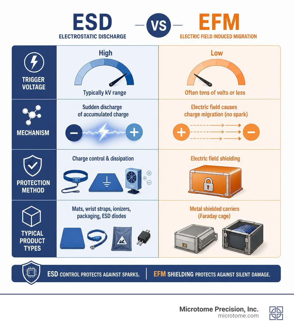
Infographic comparing ESD vs EFM: trigger voltage, mechanism, protection method, product types infographic

Evaluating ESD Products for High-Yield Semiconductor Environments

When setting up a semiconductor fabrication facility or photomask shop, selecting the correct electrostatic controls is critical to maintaining high device yields. The materials used in esd products are generally classified by their surface resistivity, which dictates how quickly they can transfer or dissipate charges.

  • Conductive Materials: Surface resistivity of less than $1 times 10^4$ ohms/sq. These materials allow charges to flow rapidly to ground. While excellent for grounding paths, raw conductive materials can cause rapid, damaging discharges if a highly charged object contacts them directly.
  • Dissipative Materials: Surface resistivity between $1 times 10^4$ and $1 times 10^{11}$ ohms/sq. These materials allow charges to flow to ground in a controlled, slower manner, preventing rapid discharge events.
  • Shielding Materials: Materials designed to attenuate electrostatic fields and direct discharges around their exterior. For standard electronic components, this is achieved via multi-layer static shielding bags. For reticles, true shielding requires a rigid, highly conductive metal enclosure.
Material Property Conductive Plastics Dissipative Plastics All-Metal Shielding (Faraday Cage)
Surface Resistivity $< 1 times 10^4$ ohms/sq $1 times 10^4$ to $1 times 10^{11}$ ohms/sq $< 1 times 10^{-2}$ ohms/sq (highly conductive)
Charge Dissipation Speed Fast Controlled / Slow Instantaneous
Electric Field Attenuation (EFM Protection) Poor (allows field penetration) Poor (transparent to transient fields) Excellent (100% attenuation)
Outgassing & Contamination Risk Medium High (due to chemical additives) Zero

For general facilities maintenance, tools, and workbench areas, engineers rely on trusted suppliers like Desco – Static Control Products and Supplies for ESD Protection to equip personnel with wrist straps, dissipative mats, and grounding cords. In local regions like Colorado, specialist suppliers such as Colorado’s Source: ESD Flooring, Installations, Certifications … and United Static Control Products: ESD Products, Home | United States provide specialized flooring systems that ensure mobile personnel maintain a resistance to ground of less than $1.0 times 10^9$ ohms and a body voltage of less than 100V.

However, when we transition from the general cleanroom floor to the lithography bay where exposed reticles are handled, standard material classifications must be re-evaluated.

Why Standard ESD Control Methods Fail to Protect Photomasks

Standard cleanroom ESD controls are designed around a single premise: preventing a high-voltage spark (ESD) from jumping from a person or a tool to a sensitive circuit. To achieve this, fabs mandate equipotential grounding via wrist straps, dissipative bench mats, and air ionizers to neutralize static on non-conductive surfaces.

While these measures successfully protect silicon wafers and printed circuit boards, they fail to protect photomasks. The primary electrostatic threat to a reticle is not a direct physical spark. Instead, it is EFM (Electric Field induced Migration).

EFM is a physical phenomenon where sub-100V electric fields polarize the sub-micron chrome or MoSi features on a quartz photomask. This polarization creates intense localized mechanical stress, causing the metal structures to migrate, deform, or peel away from the quartz substrate entirely. Because EFM is driven entirely by the presence of an electric field—and does not require a physical discharge or contact—standard dissipative plastics and grounding systems are completely transparent to this threat.

To identify where your process may be vulnerable to these hidden electrostatic fields, we offer specialized diagnostic support through our Electrostatic Protection Consultancy Service.

Cleanroom ESD Products vs. Reticle-Specific Shielding

In a typical cleanroom, active air ionization is often deployed to neutralize charges on insulative surfaces. While ionizers are useful for general contamination control, they have severe limitations when protecting reticles:

  • Slow Decay Times: Air ionizers require several seconds—sometimes up to 10 seconds or more—to neutralize a charge on a surface. During those seconds, an unshielded reticle is fully exposed to EFM-inducing fields.
  • Unbalanced Ion Output: If an ionizer’s positive and negative emitter pins become dirty or worn, the system can drift out of balance, actually depositing a net electrostatic charge onto the very items it is meant to protect.
  • Airflow Obstructions: In a busy lithography bay, automated tool hoods, SMIF indexers, and operator movements block the flow of ionized air, leaving “shadowed” zones where static fields remain completely unchecked.

Passive dissipative plastic reticle carriers are similarly inadequate. While they successfully prevent a rapid electrostatic discharge from occurring on the carrier itself, their high surface resistivity means they cannot block transient electric fields. An external electrostatic field (for instance, from a highly charged operator walking nearby) will pass directly through a dissipative plastic shell, polarizing the reticle inside.

To solve this, we design and manufacture all-metal, Faraday-cage reticle carriers that completely block external electric fields. You can explore our full range of SEMI-compliant solutions in our Products Overview.

The Physics of Electrostatic Protection: ESD vs. EFM

To understand why all-metal shielding is required for photomasks, we must look at the underlying physics.

In a standard ESD event, charge flows from an area of high potential to an area of low potential. If a person accumulates several thousand volts of static charge simply by walking across a cleanroom floor, touching an electronic component will discharge that energy in a microsecond-scale pulse.

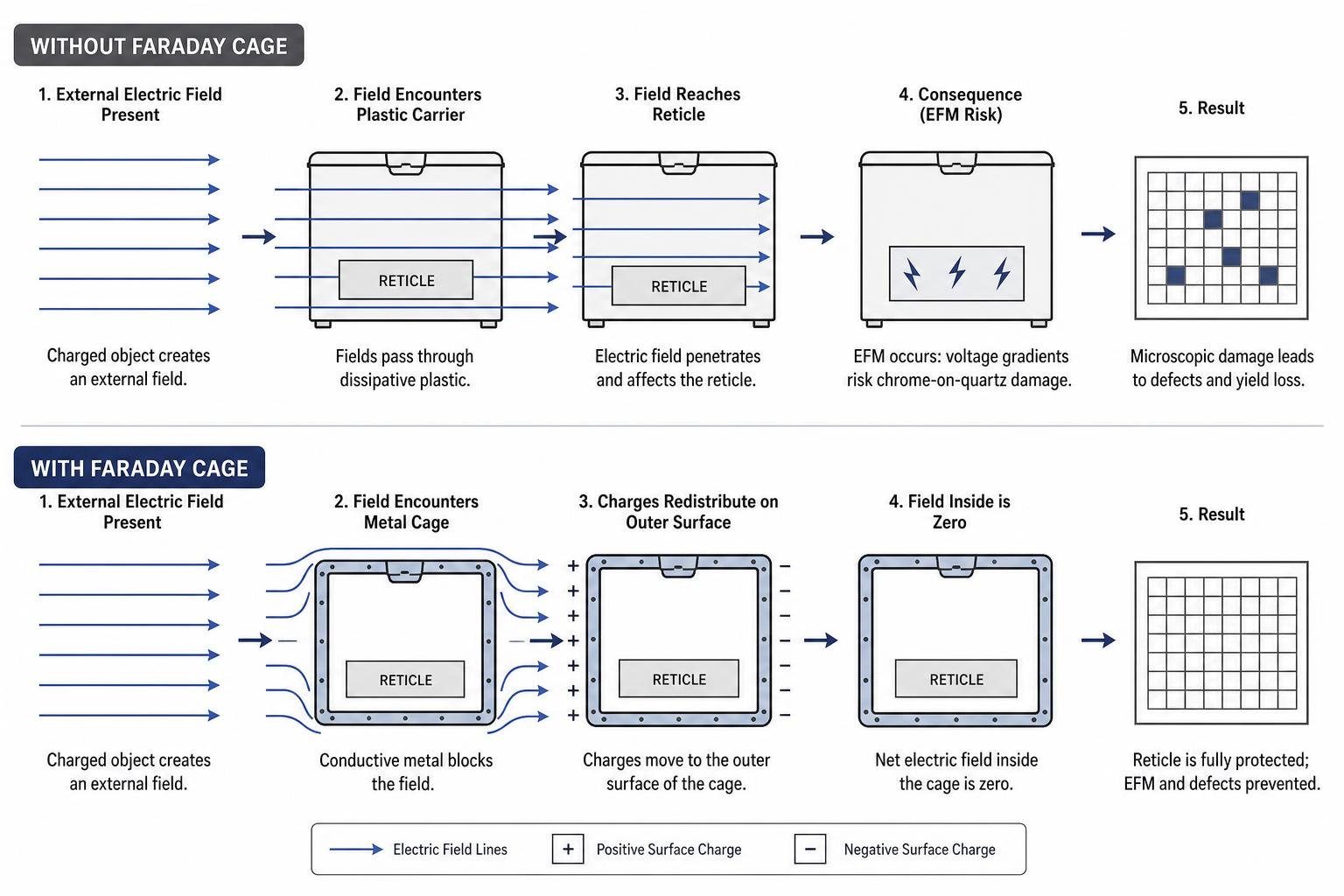
In contrast, Electric Field induced Migration (EFM) relies on field theory. According to Gauss’s Law, when an electric field encounters a hollow, highly conductive metal container—a Faraday cage—the free electrons within the metal rapidly redistribute along the outer surface of the container. This redistribution of charge creates an internal electric field that precisely cancels out the external field.

The result? The net electric field inside an all-metal container is exactly zero.
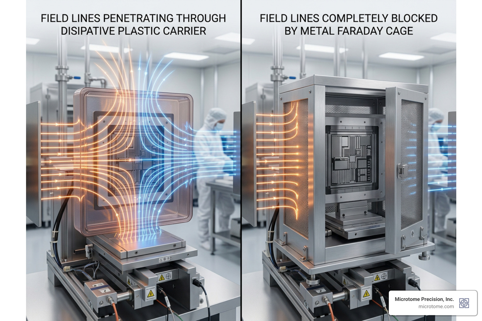
Electric field lines around a reticle inside a dissipative plastic carrier vs an all-metal Faraday cage

This electrostatic shielding is critical because the threshold for EFM damage on advanced photomasks is incredibly low. While standard integrated circuits can often withstand hundreds of volts of electrostatic stress, sub-micron reticle features can begin to migrate and degrade at field strengths equivalent to less than 100V of potential.

The international standard SEMI E163 establishes guidelines for the handling of electrostatic-sensitive items in semiconductor manufacturing, recognizing that electric fields must be managed with extreme care. Standard dissipative polymers cannot provide the rapid electron mobility required to attenuate these fields, leaving the reticle vulnerable.

The Limitations of Dissipative Plastics in Reticle Carriers

Many commercial reticle carriers, such as standard 150 mm Single Reticle SMIF pods, are constructed using static dissipative polymers with surface resistivities ranging from $10^6$ to $10^{11}$ ohms/sq. While these materials meet basic cleanroom requirements, they present serious operational trade-offs:

  1. Slow Static Decay: A typical dissipative polymer pod may have a top-to-door static decay time of approximately 10 seconds. In a automated fab, 10 seconds is an eternity. If the pod is handled or moved before this decay is complete, the reticle remains exposed to active electrostatic forces.
  2. Outgassing and Haze: Dissipative plastics rely on chemical additives, carbon powder, or inherently dissipative polymers (IDPs) to achieve their anti-static properties. Under the high-energy Deep Ultraviolet (DUV) and Extreme Ultraviolet (EUV) light used in modern lithography, these chemical additives can outgas inside the carrier. This outgassed material deposits onto the quartz mask, forming a molecular film known as “reticle haze” which ruins the mask’s optical transmission.
  3. Mechanical Degradation: Over time, repeated cleanings and exposure to cleanroom chemicals degrade the dissipative properties of plastic carriers, causing their surface resistivity to drift into the insulative range.

For these reasons, the SEMI E111 standard for single reticle SMIF pods and the SEMI E112 standard for multi-reticle cassettes demand strict mechanical and electrostatic compliance. At Microtome Precision, we bypass the limitations of dissipative plastics entirely by manufacturing our carriers out of precision-machined, high-purity aluminum. Metal does not outgas, it does not degrade, and it provides instantaneous, permanent Faraday-cage protection.

Industry Standards and Compliance for Cleanroom ESD Control

A robust ESD control program must align with recognized international and industry standards. For general electronics assembly and manufacturing, two primary standards govern facility design:

  • ANSI/ESD S20.20: This standard provides the administrative and technical requirements for establishing, implementing, and maintaining an ESD control program to protect electrical and electronic parts down to 100V Human Body Model (HBM).
  • IEC 61000-4-2: This international standard defines compliance testing for electrostatic discharge immunity at the system level. It simulates real-world ESD strikes that electronics might face during operation.

In circuit design and equipment interface protection, engineers integrate specialized transient voltage suppression (TVS) ESD protection diodes to clamp high-voltage spikes. These components are rated to dissipate severe ESD strikes per the IEC 61000-4-2 standard:

  • The ESD751 is a 1.6-pF, $pm24$-V bidirectional ESD protection diode designed for USB power delivery and general-purpose interfaces, rated to dissipate contact strikes beyond the maximum level specified in the IEC 61000-4-2 standard ($pm22$-kV contact and air gap).
  • The ESD451 is an ultra-compact 0.5-pF, 5.5-V bidirectional device in an 0201 package, rated to dissipate strikes up to $pm30$-kV (greater than Level 4 compliance).
  • The ESD701 offers an ultra-low capacitance of 0.3 pF for high-speed SerDes and HDMI 2.0 interfaces, rated up to $pm15$-kV.
  • The ESD7016 – ESD Protection Diode integrates two SuperSpeed pairs, D+, D-, and Vbus lines into a single flow-through package with an ultra-low capacitance of 0.15 pF, specifically designed to protect USB 3.0 interfaces.
  • The ESD351 is a 1.8-pF, 3.3-V unidirectional diode rated to dissipate strikes up to $pm30$-kV with extremely low clamping voltage (6.5 V at 16 A TLP).
  • The ESD321 is a 0.9-pF, 3.6-V diode rated to dissipate strikes up to $pm30$-kV, ideal for protecting USB 2.0 and Ethernet interfaces.

While these semiconductor-level diodes protect the internal circuitry of lithography tools and computers, the photomasks themselves cannot be protected by diodes. Instead, they rely on physical carriers that comply with SEMI E111 (for single reticle SMIF pods) and SEMI E112 (for multi-reticle cassettes).
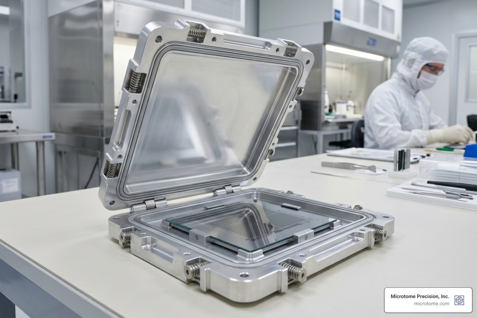
SEMI-compliant all-metal reticle carrier providing complete Faraday-cage protection

Testing and Auditing ESD Control Systems

Maintaining a compliant cleanroom requires regular auditing of all esd products. For general workbench and flooring environments, technicians use surface resistance meters to verify that mats and table surfaces remain within the dissipative range ($1.0 times 10^6$ to $1.0 times 10^9$ ohms). Electrostatic field meters are also used to detect charges on insulative plastics.

However, verifying the shielding effectiveness of a reticle carrier requires specialized testing. Standard surface resistance meters cannot accurately measure the complex geometry of a SMIF pod’s internal shielding.

To ensure that your carriers maintain physical and electrostatic compatibility with your lithography tools, we provide detailed technical specifications and verification protocols through our Compatibility Information portal.

Frequently Asked Questions about ESD Products in Lithography

Why are standard dissipative ESD products insufficient for photomask protection?

Standard dissipative ESD products are designed to slow down the flow of electric current to prevent a physical spark. However, they do not block electrostatic fields. Because photomasks are highly vulnerable to Electric Field induced Migration (EFM) at field strengths below 100V, any transient electric field will pass directly through dissipative plastics and polarize the sub-micron chrome features on the quartz mask, causing catastrophic structural degradation without any physical discharge occurring.

What is the role of SEMI E111 and E112 in reticle carrier design?

SEMI E111 defines the standardized physical dimensions, mechanical interfaces, and automation features for Single Reticle SMIF Pods, ensuring they can be seamlessly handled by robotic indexers on ASML, Nikon, and Canon lithography tools. SEMI E112 defines the standards for multi-reticle cassettes. Compliance with these standards guarantees that the carrier fits perfectly within the fab’s automated material handling systems (AMHS) while protecting the reticles from mechanical shock and contamination.

How does an all-metal Faraday cage prevent electrostatic damage?

An all-metal Faraday cage is made of highly conductive materials (such as aluminum). When an external electric field approaches the container, the free electrons in the metal instantly redistribute across the outer surface of the shell. This surface charge distribution creates an internal electric field that is equal and opposite to the external field, completely canceling it out. The electric field inside the carrier remains exactly zero, keeping the reticle perfectly safe from EFM.

Conclusion

Managing electrostatic risks in a high-yield semiconductor fab requires a clear understanding of the limits of standard esd products. While dissipative mats, grounding straps, and active ionizers are excellent for protecting wafers and general electronics, they are fundamentally incapable of shielding expensive photomasks from the destructive forces of Electric Field induced Migration (EFM).

Since 1989, Microtome Precision, Inc. has been the leading independent pioneer in reticle protection. Operating from our state-of-the-art facility in Colorado Springs, Colorado, we design and manufacture the industry’s only all-metal, SEMI E111 and E112 compliant Faraday-cage SMIF pods and cassettes. By replacing vulnerable dissipative plastics with precision-machined aluminum, we eliminate the risks of EFM, outgassing, and reticle haze.

To secure your lithography yields and upgrade your reticle transport systems, explore our Products Overview, learn about our professional Support and Repair services, or contact our engineering team today to schedule an Electrostatic Protection Consultancy Service.

The Definitive Guide to Static Dissipative Materials

What “Static Dissipative” Actually Means — and Why It Matters in the Fab

Static dissipative materials occupy a specific middle ground in electrostatic control — and choosing the wrong material category can silently damage the most expensive components in your fab.

Here is a quick-reference summary before we dive in:

Category Surface Resistivity Charge Behavior
Conductive < 1 × 10⁵ Ω/sq Charges flow rapidly to ground
Static Dissipative 1 × 10⁶ – 1 × 10⁹ Ω/sq Charges flow slowly, in a controlled manner
Antistatic ~10¹⁰ – 10¹² Ω/sq Reduces buildup but does not control decay rate
Insulative ≥ 1 × 10¹² Ω/sq Charges do not flow — static accumulates

Static dissipative materials are widely used across electronics manufacturing, cleanrooms, and semiconductor fabs to manage electrostatic discharge (ESD). They allow built-up charge to bleed off slowly and predictably — fast enough to prevent a damaging discharge, slow enough to avoid a sudden current spike that could destroy sensitive components.

Up to 33% of microchip failures have been attributed to ESD, and a properly dissipative material can reduce a 5,000-volt static charge in under 0.1 seconds. For most ESD workspaces, that performance is exactly what is needed.

But for semiconductor reticle protection, the picture is more complicated.

Standard ESD controls — including static-dissipative and conductive plastics — address the wrong threat. Reticles face a distinct electrostatic failure mode called EFM (Electric Field induced Migration) that occurs at far lower stress levels than conventional ESD. Microtome Precision’s research team characterized EFM in 2003, and it fundamentally changes how electrostatic protection for photomasks must be designed.

I’m Matt Pilarski, President of Microtome Precision, Inc., the longest-established independent designer and manufacturer of reticle carriers in the semiconductor industry. My work over more than three decades has centered on understanding exactly where static dissipative plastics fall short — and what true electric-field shielding requires. In the sections that follow, we’ll build a precise, technically grounded picture of the full static-dissipative material landscape and explain where its limits begin.

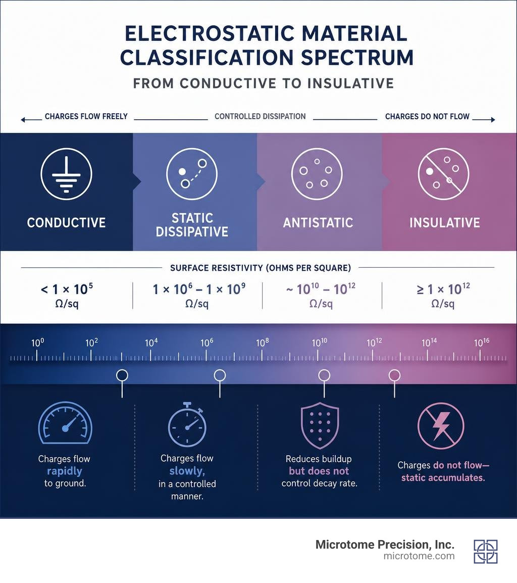
Electrostatic material classification spectrum from conductive to insulative with resistivity ranges infographic

Defining Static Dissipative Materials and Electrical Resistance Ranges

To understand how a static dissipative material works, we have to look at how electrical resistance is measured and defined. At its core, electrical resistance is a material’s natural opposition to the flow of an electric current. When we discuss materials used to control static electricity, we primarily classify them using two metrics: surface resistivity and volume resistivity.

Surface resistivity testing on advanced polymer samples in a laboratory

Surface resistivity measures the electrical resistance across the surface of a material. It is expressed in ohms per square ($Omega$/sq). The “per square” unit is a mathematical convention; because the path’s length and width cancel each other out in a square geometry, the resistivity value remains identical regardless of the size of the square being measured.

Volume resistivity, on the other hand, measures the resistance of a material through its entire thickness. It is expressed in ohm-centimeters ($Omega$-cm) and represents the material’s bulk resistance.

The industry-accepted boundary for a static dissipative material is a surface resistivity between $1 times 10^6$ and $1 times 10^9$ ohms per square. In some broader contexts, materials with a surface resistivity up to $1 times 10^{11}$ ohms per square are still categorized as dissipative, but for critical cleanroom and manufacturing environments, the tighter $10^6$ to $10^9$ range is the benchmark.

To put this in perspective, let us look at how the entire electrostatic spectrum is classified:

For a deeper dive into these classifications, you can read the technical breakdown provided by Duracote on What is Anti Static vs. Static Dissipative? | Learn About an ESD ….

Measuring Surface Resistivity in Static Dissipative Polymers

To verify that a polymer is truly static dissipative, metrology teams rely on standardized testing methods, most notably ASTM D257. Measuring the resistivity of compounded thermoplastics requires specialized equipment and strict adherence to protocol to avoid false readings.

A standard measurement setup uses a high-quality ohmmeter connected to a concentric ring probe or parallel bar electrodes. To ensure accurate contact, the electrodes must be placed under a specific load. Without sufficient contact pressure, microscopic air gaps between the electrode and the polymer surface will act as insulators, artificially inflating the resistance reading.

Furthermore, polymer compounding plays a massive role in how these measurements behave. Many static dissipative plastics are made by compounding an insulative base polymer (like PEEK, polycarbonate, or POM) with conductive additives such as carbon powder, carbon fibers, or carbon nanotubes. If these additives are not uniformly dispersed, the material will exhibit “hot spots” of high conductivity alongside highly insulative pockets. Testing must be performed at multiple locations across the material to guarantee a consistent, homogeneous dissipative path.

Comparing Conductive, Insulative, Antistatic, and Static Dissipative Classifications

When designing a cleanroom or assembly area, choosing the right material class is a balancing act between safety and speed. A material that is too conductive can cause a rapid, spark-like discharge, while a material that is too insulative will hold onto its charge indefinitely.

The table below illustrates how these material classes handle charge decay and triboelectric charging:

Material Class Typical Surface Resistivity ($Omega$/sq) Charge Decay Velocity Triboelectric Generation Risk Common Examples
Conductive $< 1 times 10^5$ Instantaneous (< 0.01s) Low (if grounded) Metals, carbon-filled rubber
Static Dissipative $1 times 10^6$ to $1 times 10^9$ Controlled (< 0.1s) Very Low Staticide SpecMat H, ESD vinyl
Antistatic $10^{10}$ to $10^{12}$ Very Slow / Variable Low Topical anti-static sprays, cleanroom garments
Insulative $ge 1 times 10^{12}$ Extremely Slow / None High Standard plastics, quartz, glass

In general ESD workspaces, the primary goal is to prevent triboelectric charging while providing a safe, controlled path to ground. If an operator carrying a static charge touches a conductive surface, the charge dumps instantly, potentially melting sub-micron gates on a silicon wafer. If that same operator touches a static dissipative surface, the charge is bled off in a controlled manner, neutralizing the voltage difference without a sudden, destructive current spike.

Why Static Dissipative Materials are Used in General ESD Workspaces

In standard ESD Protected Areas (EPAs), static dissipative materials are the gold standard for work surfaces, floor runners, and hand tools. The primary benefit is their predictable charge decay rate. For instance, high-performance dissipative mats are engineered to dissipate a 5,000-volt static charge in less than 0.1 seconds.

Workbenches are frequently outfitted with dual-layer elastomers such as the Staticide® Dualmat™ Static Dissipative Mat, which features a static-dissipative top layer to handle components safely and a conductive bottom layer to establish a reliable path to ground. Similarly, three-layer materials like Staticide® TriMat use a conductive middle layer sandwiched between two dissipative layers to provide cushioned physical protection alongside electrical grounding.

For cleanroom flooring, facilities often utilize products like the StaticWorx Eclipse Electrically Conductive EC Rubber or Aisle-Safe SD and EC Rubber Runners & Mats to create a continuous, grounded walking surface. These materials prevent personnel from generating high walking body voltages, keeping the environment safe for general electronic assembly.

However, there is a hard limit to what these materials can achieve.

While a static-dissipative floor or mat is excellent for protecting populated printed circuit boards (PCBs) or general electronic components, these materials are fundamentally insufficient for protecting photomasks (reticles) in lithography environments. The physics governing reticle degradation are entirely different from the physics of general ESD, as we will explore next.

The Limits of Static Dissipative Plastics in Semiconductor Photomask Protection

In semiconductor manufacturing, the photomask—or reticle—is the master template used to print billions of microscopic transistors onto silicon wafers. A single high-end EUV or optical reticle can cost hundreds of thousands of dollars. Protecting these assets from contamination and electrostatic damage is a top priority for any fab.

Semiconductor reticle carrier being handled in a cleanroom environment

Unfortunately, many fab engineers mistakenly assume that because a reticle carrier (such as a SMIF pod or cassette) is made from “ESD-safe” static dissipative plastic, the reticle inside is protected. This is a dangerous misconception.

While static dissipative plastics prevent the accumulation of high triboelectric charges on the carrier itself, they are completely transparent to electrostatic fields. If an external electrostatic charge is brought near a plastic SMIF pod, the resulting electric field passes directly through the plastic shell. It reaches the reticle inside, creating a localized electric field that can destroy the mask without a single spark ever occurring.

Electrostatic Field Hazards and EFM in Lithography Cleanrooms

The dominant electrostatic risk to semiconductor reticles is not Electrostatic Discharge (ESD); it is Electric Field induced Migration (EFM).

Discovered and characterized by Microtome Precision in 2003, EFM is a phenomenon where sub-micron metal features (such as chromium or ruthenium lines) on a quartz reticle substrate are physically pulled, distorted, or migrated by the force of an external electric field. EFM occurs at electrostatic stress levels far lower than the thresholds required to cause a conventional ESD event.

Because static-dissipative plastics allow electric fields to penetrate the carrier interior, they cannot prevent EFM. The only way to completely eliminate EFM risk is to block the electric field entirely. This requires a physical phenomenon known as a Faraday cage.

An all-metal, Faraday-cage reticle carrier provides absolute shielding. When an external electric field encounters an all-metal pod, the mobile electrons in the metal shell instantly redistribute along the outer surface, perfectly canceling out the electric field inside the cavity. The interior field remains exactly zero.

At Microtome Precision, Inc., we design and manufacture SEMI E111 (single reticle pod) and SEMI E112 (multi-reticle cassette) compliant, all-metal Faraday-cage carriers. Our proprietary research demonstrates that relying on static-dissipative or conductive plastics for reticle protection actually increases EFM risks by failing to shield the mask from transient cleanroom fields. To understand how we apply these principles to protect your lithography yields, you can explore our specialized Electrostatic Protection Consultancy Service or view our full range of Products.

Industry Standards and Testing Methods for ESD-Safe Environments

Maintaining an ESD-safe fab requires continuous testing and compliance verification. Several key standards govern how static dissipative materials are evaluated and certified in industrial settings:

Verifying Compliance in Semiconductor Manufacturing Facilities

To verify compliance with these standards, metrology teams perform regular testing of all ESD control elements. The two most common testing protocols are:

  1. Resistance-to-Ground (RTG): This test measures the electrical resistance between a specific point on a work surface or floor and the facility’s master ground. It ensures that any static charge deposited on the surface has a clear, uninhibited path to ground.
  2. Resistance Top-to-Top (RTT): This test measures the resistance between two distinct points on the same surface. It is used to verify the uniformity of a dissipative material, ensuring there are no insulative dead zones.

In our local semiconductor hub of Colorado, facilities must maintain strict compliance with these standards. For local testing, certification, and specialized installation protocols, regional fabs often work with local experts like Colorado’s Source: ESD Flooring, Installations, Certifications and … and ESD Flooring Denver – Colorado Concrete Repair to ensure their cleanroom floors meet the rigorous requirements of ANSI/ESD S20.20.

Frequently Asked Questions about Static Dissipative Materials

What is the exact resistance range of a static dissipative material?

To qualify as static dissipative, a material must have a surface resistivity between $1 times 10^6$ and $1 times 10^9$ ohms per square (or a resistance-to-ground in the same range). This specific window allows charges to decay in a controlled manner, preventing both the rapid discharge associated with conductive materials and the charge retention associated with insulative materials.

How does a static dissipative material differ from an antistatic material?

The term “antistatic” refers to a material’s ability to resist the generation of static charges via friction (triboelectric charging). An antistatic material does not necessarily provide a fast or controlled path to ground; it simply prevents charge from building up in the first place. A static dissipative material, however, is specifically engineered to conduct charges to ground at a slow, controlled, and mathematically predictable rate.

Why are static dissipative plastics insufficient for protecting semiconductor reticles?

Static dissipative plastics are transparent to electrostatic fields. While they prevent static charges from building up on the carrier itself, they allow external electric fields from cleanroom operators, machinery, or ionized air to pass directly through to the reticle inside. These fields cause Electric Field induced Migration (EFM), which damages the sub-micron features on the mask. Only an all-metal Faraday cage can shield a reticle from these fields.

Conclusion

Static dissipative materials are a critical component of any comprehensive ESD control program. By keeping surface resistivity within the $10^6$ to $10^9$ ohms per square range, these materials provide a safe, controlled path to ground for transient charges, protecting sensitive electronic assemblies across the fab.

But as we have discussed, general ESD protection is not reticle protection. When it comes to safeguarding highly sensitive, expensive photomasks, static dissipative plastics fall short because they cannot block the electrostatic fields that cause EFM.

Since 1989, Microtome Precision, Inc. has been dedicated to a single mission: “Reticle protection IS our business.” From our facility in Colorado Springs, Colorado, we design and manufacture the industry’s only all-metal Faraday-cage SMIF pods and cassettes to provide absolute electrostatic field shielding.

To ensure your carriers continue to provide maximum protection and meet strict SEMI E111 and E112 standards, we also offer a comprehensive recertification program. Learn more about our Support and Repair (R&R) Services or contact our team directly through our Contact Page to discuss how we can help you eliminate EFM risks in your lithography bay.

Electrostatic Discharge Meaning: Terms Demystified

What Electrostatic Discharge Meaning Really Tells Us — And What It Misses

Understanding the electrostatic discharge meaning is straightforward at first glance:

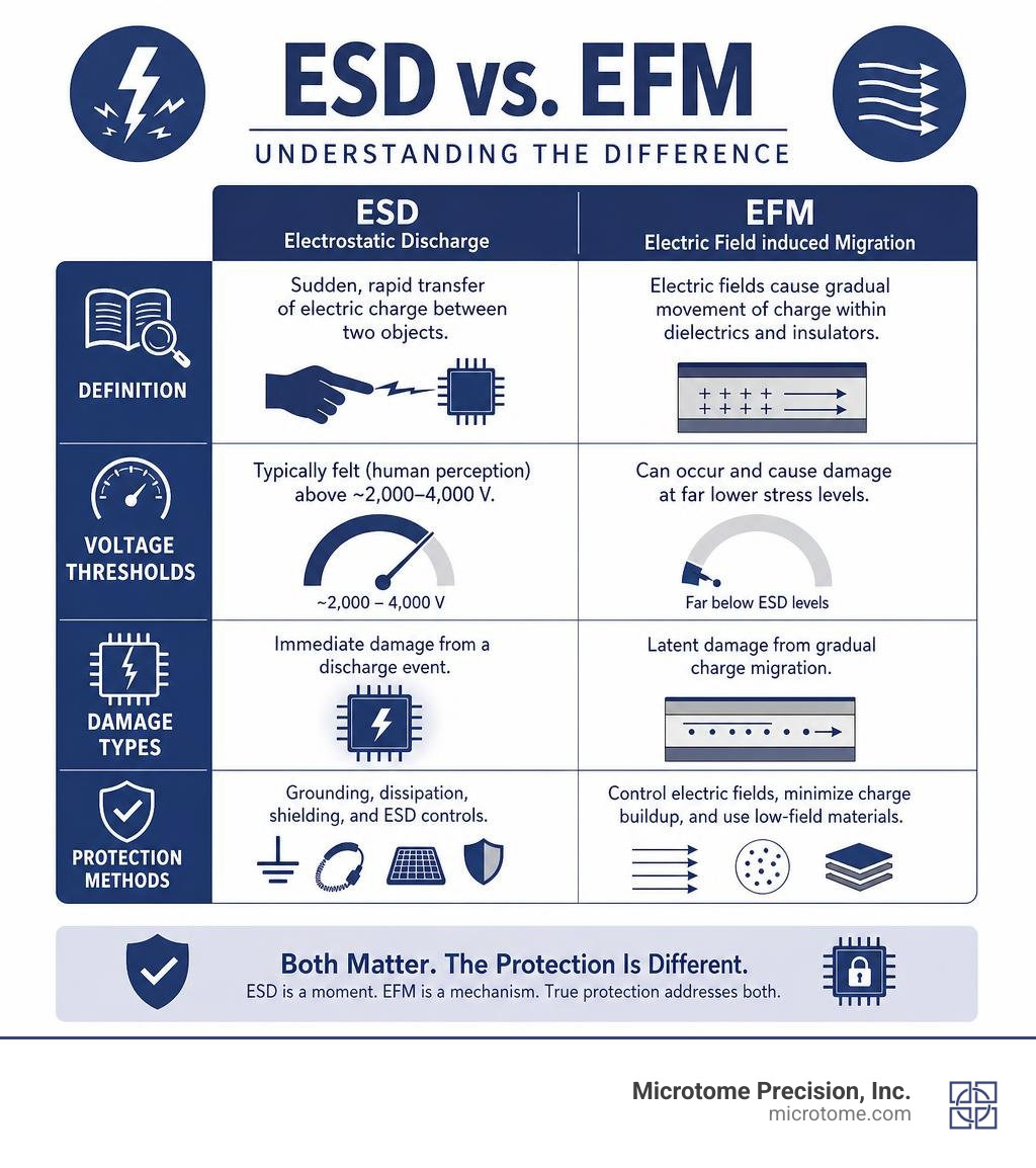
Electrostatic discharge (ESD) is the sudden, rapid transfer of electric charge between two objects at different electrical potentials — through direct contact, an arc, or dielectric breakdown.

Here is a quick-reference summary:

Term Plain-language meaning
Electrostatic charge A buildup of electrical charge on a surface
Discharge The sudden release of that stored charge
ESD event The moment charge jumps between two objects
Damage threshold Some components fail at as little as 30 V
Typical human perception You feel a shock only above ~2,000–4,000 V

The tricky part? ESD is only part of the electrostatic hazard picture — especially in semiconductor lithography.

Walking across a carpet can generate up to 35,000 volts at low humidity. Yet most people feel nothing until thousands of volts have already built up. For general electronics, standard ESD controls — grounding, dissipative mats, wrist straps — do a reasonable job.

But for photomasks (reticles), the situation is fundamentally different. A reticle can cost over a million dollars and take weeks to qualify. The electrostatic threat that matters most for reticles is not a dramatic discharge event. It is a far subtler mechanism called EFM (Electric Field induced Migration) — and it operates at stress levels far below what conventional ESD protection is designed to stop.

That distinction is what this guide is built around.

I’m Matt Pilarski, President of Microtome Precision, Inc., where we have specialized in reticle carrier design and the electrostatic discharge meaning as it applies to photomask protection since 1989. Microtome’s research team characterized EFM in 2003, identifying a reticle failure mode that standard ESD frameworks simply do not address — and everything we build is designed around closing that gap.

Infographic comparing ESD and EFM: definitions, voltage thresholds, damage types, and protection methods infographic

Easy electrostatic discharge meaning word list:

The Technical Electrostatic Discharge Meaning in Semiconductor Environments

To understand how electrostatic hazards compromise a cleanroom, we must look at the formal physics definition. According to the International Electrotechnical Commission (IEC), an electrostatic discharge is the transfer of electric charge between bodies of different electrostatic potentials when they are brought close together or when the dielectric between them breaks down.

In a standard fab, this means a sudden, high-speed flow of current. When two materials with different potentials approach one another, the electric field between them intensifies. If this field strength exceeds the dielectric strength of the surrounding medium (which is approximately 4 to 30 kV/cm for dry air), the air ionizes. This creates a highly conductive plasma path—often visible as a spark—allowing rapid charge equalization.

However, in advanced semiconductor manufacturing, focusing only on visible sparks is a dangerous mistake. Many discharges occur well below the human threshold of perception (typically 2,000 to 4,000 volts). A technician can touch a carrier, cause a 100-volt discharge, and remain completely unaware of the event. Yet, that faint discharge is more than enough to destroy sub-micron structures.

To fully grasp how these events are quantified and managed in the fab, engineers must familiarize themselves with standard verification procedures, which we discuss in detail in An Essential Guide to ESD Test Basics.

Mechanisms of Static Charge Generation and ESD Events

Before an ESD event can occur, an electrostatic charge must first accumulate. In any manufacturing environment, static charge is generated constantly through everyday operations. Understanding how these charges accumulate is the first step toward controlling them.

Tribocharging and Electrostatic Induction

The most common mechanism of charge generation is triboelectric charging (or tribocharging). As defined in EOS/ESD Fundamentals Part 1 | EOS/ESD Association, Inc., tribocharging is the creation of electrostatic charge by the contact and separation of materials.

When two materials are pressed together, their surface atoms interact, and electrons migrate from one material to the other based on their position in the triboelectric series. When they are quickly separated, one material retains a net positive charge (having lost electrons), while the other gains a net negative charge.

tribocharging mechanism contact and separation

Common cleanroom examples of tribocharging include:

The second major mechanism is electrostatic induction. This occurs when a pre-existing charged object is brought near an ungrounded conductor. The electric field from the charged object forces the mobile electrons in the conductor to redistribute, creating highly charged regions of opposite polarity on the conductor’s surface—even though its net charge remains zero. If that conductor then contacts a ground or another object, a sudden discharge occurs. This induction effect is why simply keeping “non-grounded” tools near sensitive areas is highly hazardous.

Standard ESD Testing Models and Susceptibility

To evaluate how sensitive electronic components and photomasks are to these charges, the industry relies on standardized test models. These models simulate real-world discharge paths to establish a device’s withstand voltage:

For a deeper dive into how these models are applied in practice, read The Ultimate Guide to ESD Safe Products.

Why Standard ESD Protection Fails for Photomasks: The Threat of EFM

In general electronics manufacturing, ESD damage usually manifests as physical destruction: oxide rupture, junction filamentation, or metal lines melting. These are often categorized as either catastrophic failures (the device fails immediately) or latent defects (the device is weakened and fails prematurely in the field).

For photomasks (reticles), however, the threat profile is entirely different. Standard ESD protection practices, such as wearing grounded wrist straps or using static-dissipative plastic carriers, are designed to prevent sudden discharges. But they do absolutely nothing to protect against a far more insidious phenomenon: Electric Field induced Migration (EFM).

The Electrostatic Discharge Meaning vs. Electric Field Induced Migration (EFM)

While the electrostatic discharge meaning focuses on the flow of current during a discharge, EFM is driven entirely by the presence of an electric field.

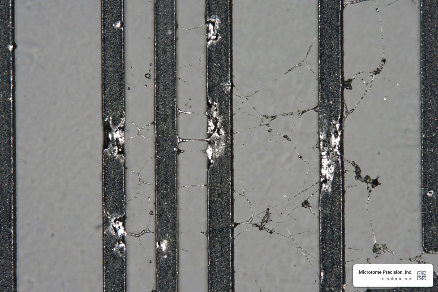
EFM damage on a photomask reticle chrome line

First characterized by our research team at Microtome Precision in 2003, EFM occurs when a photomask is exposed to a localized electrostatic field. Reticles consist of sub-micron chrome features deposited on a non-conductive quartz substrate. When an external electric field penetrates the carrier, it induces a massive potential gradient across these tiny chrome lines.

Because the chrome lines are incredibly narrow and separated by microscopic gaps, even a relatively low external voltage can create an electric field strength of several million volts per meter between adjacent chrome structures. Under this intense electrostatic field stress, chrome atoms physically migrate across the quartz gaps. This migration causes:

  1. Progressive degradation of the sub-micron chrome lines.
  2. The formation of microscopic chrome “bridges” or filaments between lines.
  3. Severe lithographic printing defects, destroying wafer yield long before any physical “spark” or ESD event ever occurs.

The Limitations of Dissipative Plastics and Ionizers

Many fabs mistakenly believe that using static-dissipative or “conductive” plastic SMIF pods and cassettes provides adequate protection for reticles. This is a dangerous misconception.

Static-dissipative polymers are designed to slowly bleed off static charges to ground. However, they are still plastics. They do not block electric fields. When a charged object (like a technician’s sleeve or a plastic tool) comes near a dissipative plastic carrier, the external electric field passes directly through the plastic wall and reaches the reticle inside, inducing EFM.

Furthermore, these engineered plastics often rely on additives that can outgas over time in the cleanroom environment. This outgassing leads to molecular contamination on the reticle surface, resulting in progressive “haze” defects when exposed to high-energy lithography light sources.

Feature Static-Dissipative Plastics All-Metal Faraday Cages
ESD Prevention Prevents rapid discharge only Prevents rapid discharge
Electric Field Shielding Poor (fields pass straight through) Absolute (100% attenuation)
Outgassing Risk High (additives cause reticle haze) Zero (pure, cleanroom-grade metals)
Durability Degrades over time and washes Indefinite life, fully recertifiable

To learn more about preventing these issues, consider utilizing our specialized Electrostatic Protection Consultancy Service.

Implementing True Electrostatic Shielding in Lithography Fabs

To protect costly photomasks from both ESD and EFM, fabs must move beyond basic grounding and implement true electrostatic shielding.

Faraday Cage Principles for Reticle Protection

A Faraday cage is an enclosure formed by conductive material. When an external electric field encounters a highly conductive metal surface, the free electrons within the metal rapidly redistribute. This charge redistribution creates an internal electric field that is equal and opposite to the external field, completely canceling it out. As a result, the net electric field inside the enclosure is exactly zero.

Faraday cage electric field shielding diagram

By housing a reticle inside an all-metal, highly conductive enclosure, you ensure that external electric fields—regardless of their strength—cannot penetrate the carrier. This eliminates the voltage gradients across the chrome-on-quartz features, preventing EFM entirely.

This shielding principle is recognized by international standards bodies. To ensure maximum yield protection, reticle carriers should comply with SEMI standards, specifically SEMI E111 (specifications for single reticle SMIF pods) and SEMI E112 (specifications for multi-reticle cassettes).

The Role of All-Metal Carriers in Preventing EFM and ESD

At Microtome Precision, Inc., we design and manufacture all-metal reticle carriers (cassettes and SMIF pods) engineered specifically to act as robust Faraday cages.

Constructed from precision-machined, cleanroom-grade aluminum, our carriers provide absolute electric field shielding. Because they are entirely metallic, they do not outgas, eliminating the risk of chemical contamination and haze on your photomasks. They are designed to integrate seamlessly with both modern and legacy lithography tools, maintaining strict compliance with SEMI standards.

To keep your fleet of carriers performing at their peak, we also offer a comprehensive cleanroom-based recertification program. Learn more about our maintenance options by visiting our Support and Repair page, or explore our full lineup of Products.

Frequently Asked Questions about Electrostatic Discharge Meaning

What is the exact electrostatic discharge meaning in cleanrooms?

In a semiconductor cleanroom, the electrostatic discharge meaning refers to the rapid, uncontrolled transfer of static charge between tools, operators, and silicon wafers or photomasks. Because cleanroom air is kept at a strictly controlled relative humidity (typically 30% to 50% to prevent condensation and microbial growth), static charges generate easily and dissipate slowly. ESD in the cleanroom not only destroys sensitive microstructures directly but also causes Electrostatic Attraction (ESA), pulling airborne particles onto wafers and reticles, which leads to severe imaging defects.

How does EFM differ from standard ESD?

Standard ESD requires a physical discharge path—a spark or current flow—to cause damage. EFM (Electric Field induced Migration) requires no physical contact or discharge. It is caused purely by the stress of an external electrostatic field penetrating a carrier. This field forces the chrome atoms on a reticle to migrate across the quartz substrate, degrading sub-micron lines at voltage levels far below the threshold of standard ESD events.

Why are static-dissipative plastics risky for reticles?

Static-dissipative plastics are excellent for general-purpose ESD workbenches, but they are inadequate for reticle protection. They do not block electric fields, allowing EFM-inducing fields to pass directly through to the photomask. Additionally, the chemical additives used to make these plastics dissipative can outgas in the fab, depositing carbon-based contaminants on the reticle that cook under lithography lasers, creating progressive reticle haze.

Conclusion

Demystifying the electrostatic discharge meaning reveals that managing electrostatic hazards in a semiconductor fab requires looking far beyond simple sparks. While standard ESD protection is sufficient for general electronics, photomasks demand a fundamentally different approach. The threat of Electric Field induced Migration (EFM) means that static-dissipative plastics and air ionizers are simply not enough—and can often introduce new contamination risks.

Protecting your lithography yield requires absolute electrostatic shielding. Since 1989, Microtome Precision, Inc. has been the independent leader in reticle protection. Our all-metal, SEMI-compliant SMIF pods and cassettes provide a true Faraday cage to eliminate both ESD and EFM, ensuring your photomasks remain pristine.

To secure your lithography process and protect your tooling investments, contact our engineering team in Colorado Springs today. Explore our Products or reach out to our Support and Repair division to discuss how we can help you eliminate electrostatic yield loss.

^