
An Essential Guide to ESD Test Basics
Why ESD Testing Is Critical for Electronics and High-Value Components
An ESD test is a structured procedure used to determine how well a semiconductor device, electronic system, or facility can withstand electrostatic discharge events without suffering damage or performance loss.
Here’s a quick summary of what ESD testing covers:
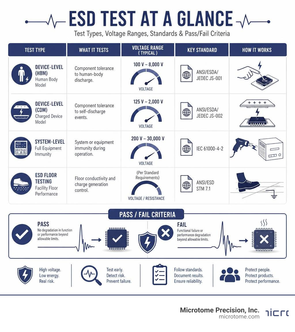
| ESD Test Type | What It Tests | Common Standard |
|---|---|---|
| Device-level (HBM) | Component tolerance to human-body discharge | ANSI/ESDA/JEDEC JS-001 |
| Device-level (CDM) | Component tolerance to self-discharge | ANSI/ESDA/JEDEC JS-002 |
| System-level | Full equipment immunity during operation | IEC 61000-4-2 |
| ESD floor testing | Facility floor conductivity and charge generation | ANSI/ESD STM 7.1 |
ESD events can reach thousands of volts — yet remain low enough in total energy that a person barely notices them. That combination is exactly what makes them so dangerous to electronics. The voltage is high enough to punch through microscopic circuit structures, but the event is invisible and silent.
The damage isn’t always immediate. ESD can cause latent defects — hidden weaknesses that cause a component to fail weeks or months after the discharge event. In high-stakes environments like semiconductor fabrication, where a single reticle can cost over a million dollars, even a latent defect can have devastating consequences.
Understanding ESD testing — what it measures, how it’s performed, and what the results mean — is the foundation of any serious static control program.
I’m Matt Pilarski, President of Microtome Precision, Inc., where we’ve been protecting reticles from electrostatic damage since 1989, and our research team discovered EFM (Electric Field induced Migration), a reticle failure mode triggered at far lower electrostatic stress than conventional ESD test thresholds. That background shapes everything in this guide.
What is an esd test and Why Does It Matter?
At its core, an esd test is the process of applying a series of controlled, high-voltage pulses to a component, system, or material to replicate real-world static discharge events. By doing this, engineers can evaluate how much electrical stress an object can handle before it fails or degrades.
To understand why this is so critical, we have to look at the physics of static electricity. An electrostatic discharge is a sudden, rapid transfer of electric charge between two objects at different electrical potentials. It is a classic low-energy event that packs a massive high-voltage punch. While you might not feel a static shock until it reaches about 3,000 volts, delicate semiconductor junctions can be permanently destroyed by a mere fraction of that voltage.
When an unprotected device experiences an ESD event, the results generally fall into two categories:
- Immediate Catastrophic Failure: The component fails right away. This is actually the “convenient” failure mode because you catch it during quality control testing on the factory floor.
- Latent Defects: The component is wounded but still functions. It passes initial factory testing, only to fail unexpectedly months later in the hands of an end-user. This is an engineering nightmare that leads to high warranty return costs and damaged brand reputation.
To prevent these issues, manufacturers use standard testing protocols to classify device sensitivity. If you want to dive deeper into the fundamentals of how semiconductor tolerance is measured, you can read more about What is Electrostatic discharge (ESD) testing.
For organizations struggling to manage these invisible threats, utilizing an Electrostatic Protection Consultancy Service can help identify vulnerabilities in your workflows and design custom mitigation strategies before static issues impact your bottom line.
Device-Level vs. System-Level ESD Testing
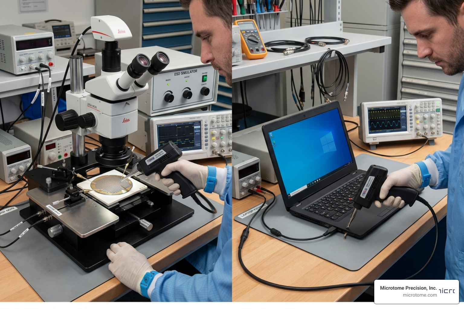
A common point of confusion for engineers is the difference between device-level and system-level testing. They serve entirely different evaluation targets, use different equipment, and apply completely different pass/fail criteria.
- Device-Level Testing: This evaluates individual, unmounted semiconductor components (like ICs, transistors, and diodes) during manufacturing, assembly, and packaging. The goal is to ensure the component can survive the automated handling and assembly processes. The pass/fail criteria are strictly parametric—meaning if the device’s electrical characteristics shift beyond specified limits, it is considered a failure.
- System-Level Testing: This evaluates a complete, fully operational electronic product (such as a laptop, a medical monitor, or an automotive dashboard) in its final end-user environment. The goal is to verify functional immunity—meaning the system can withstand a static shock to its chassis, buttons, or ports and continue operating normally, or recover gracefully without user intervention.
Because we design systems to integrate smoothly with diverse components, verifying Compatibility between your protective hardware and the system-level environment is vital. To learn more about how specialized labs conduct these evaluations, you can explore the insights provided by an ESD Testing – Applied Technical Services facility.
Device-Level esd test Models: HBM, CDM, and MM
Device-level testing relies on three historical mathematical models to simulate different real-world charging and discharging scenarios.
Human Body Model (HBM)
The Human Body Model simulates a human being accumulating static charge (for example, by walking across a carpet) and then touching a pin of a sensitive device. It is modeled by charging a 100 pF capacitor and discharging it through a 1.5 kΩ resistor into the device under test (DUT).
A typical HBM waveform has a rise time of 2–10 ns, a peak current of 0.67 amps per kilovolt of stress, and a double-exponential decay with a total width of roughly 200 ns. The primary standard for this is the joint JEDEC/ESDA standard. For complete technical parameters, you can review the official document For Electrostatic Discharge Sensitivity Testing.
Charged Device Model (CDM)
The Charged Device Model simulates a scenario where the device itself becomes charged (perhaps by sliding down an automated part feeder) and then suddenly contacts a grounded conductive surface. Because there is no current-limiting resistor in this path, CDM events are incredibly fast and violent.
The discharge duration is often less than one nanosecond, with peak currents reaching tens of amperes. This is the most common cause of ESD failures in modern automated manufacturing. You can find detailed descriptions of these mechanisms in the Basics of Electrostatic Discharge training materials.
Machine Model (MM)
The Machine Model simulates discharge from a charged tool or mechanical equipment. Historically, it was modeled using a 200 pF capacitor with no series resistor, delivering an oscillatory waveform. However, because of extreme variations in tester inductance and poor reproducibility, the industry has largely phased out MM for qualification, preferring HBM and CDM which cover more than 99% of field failure signatures.
| Parameter | Human Body Model (HBM) | Charged Device Model (CDM) | Machine Model (MM) Historical |
|---|---|---|---|
| Equivalent Capacitance | 100 pF | Variable (device dependent) | 200 pF |
| Equivalent Resistance | 1.5 kΩ | < 1 Ω (direct discharge) | 0 Ω |
| Typical Rise Time | 2 to 10 ns | < 1 ns | Oscillatory, rapid rise |
| Peak Current | 0.67 A per kV | Very high (tens of Amps) | High, highly variable |
| Primary Standard | ANSI/ESDA/JEDEC JS-001 | ANSI/ESDA/JEDEC JS-002 | AEC-Q101-002 |
System-Level esd test Standards and Waveforms
System-level testing simulates a much harsher environment. Unlike a loose chip on a tray, a finished product has to survive real-world abuse. System-level waveforms involve much larger peak currents and faster rise times.
The dominant international standard for commercial electronics is IEC 61000-4-2. This standard defines the testing parameters for equipment exposed to human-metal discharges (where a person holding a metal tool, like a key or screwdriver, discharges into a device).
Other critical system-level standards include:
- ISO 10605: Used for automotive electronics testing, where testing is conducted from 2 kV up to 25 kV in both polarities to account for the unique environments inside vehicles.
- MIL-STD-461 CS118: The military standard for ESD compliance, with test levels reaching up to 15 kV.
The latest updates, specifications, and measurement uncertainty guidelines are detailed in the IEC 61000-4-2:2025 standard, which remains the global benchmark for system compliance.
How to Test an ESD Floor for Facility Compliance
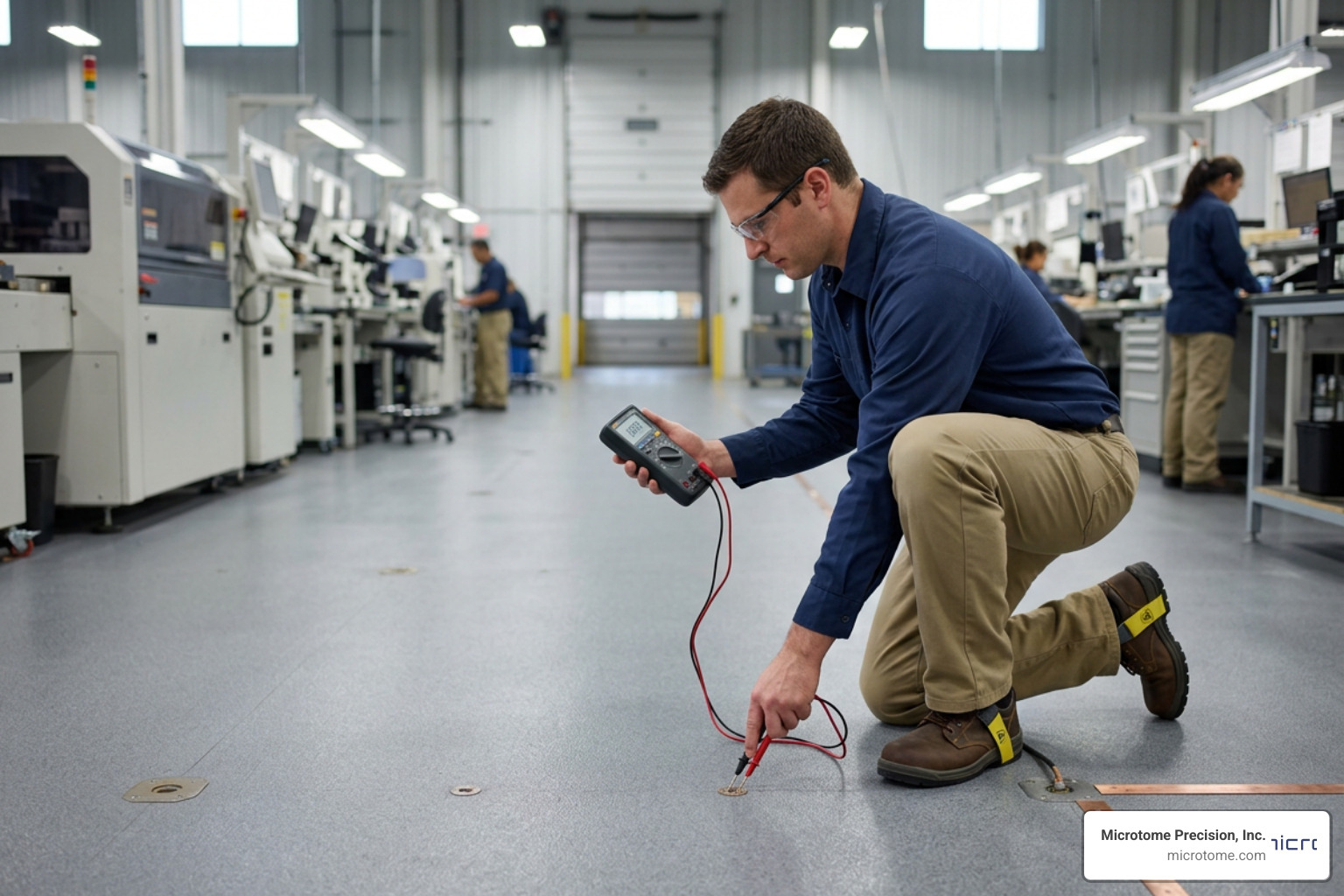
You can have the most robust ESD-protected components in the world, but if your manufacturing floor is generating thousands of volts of static electricity, you are fighting a losing battle. Testing and maintaining your ESD flooring is an absolute prerequisite for facility compliance.
There are three primary methods used to evaluate an ESD floor:
1. Electrical Resistance Test (ANSI/ESD STM 7.1)
This is the most common method of qualifying and verifying an ESD floor. It measures the resistance between the floor surface and a known grounding point (resistance-to-ground), or between two points on the floor surface (point-to-point resistance).
To conduct this test, you place standard five-pound, 2.5-inch diameter electrodes on the floor and apply a test voltage (typically 10V or 100V).
- For electronics manufacturing environments: The floor must measure < 1.0 x 10E9 ohms.
- For end-user environments (like flight towers or server rooms): The floor should measure > 1.0 x 10E6 and < 1.0 x 10E9 ohms to ensure safety from electrical shock while still dissipating static.
2. Walking Body Voltage Test (ANSI/ESD STM97.2)
Resistance testing alone does not tell the whole story because it doesn’t measure how much charge a human actually generates while moving. The walking body voltage test measures the actual static voltage accumulated on a person’s body while walking on the floor wearing specific footwear.
- For electronics manufacturing and handling facilities: The floor/footwear system should generate < 100V.
- For end-user environments: The generated body voltage must remain < 500V.
Because different shoe soles generate different levels of friction, this test should be repeated with every type of footwear permitted in your cleanroom or factory.
3. Static Control Audit
A comprehensive static control audit is a periodic, third-party evaluation of your entire ESD control program. This audit verifies that your floors, wrist straps, ionizers, and workstations are working in harmony. If you need assistance setting up these testing protocols or verifying your facility, you can consult with Professional ESD Testing Services | ETS Laboratory to ensure your cleanroom meets rigorous standards.
Equipment, Setup, and Execution of ESD Testing
To conduct system-level compliance testing, a highly controlled environment is required. The test setup consists of several specialized pieces of equipment working together.
The ESD Simulator (ESD Gun)
The primary tool is an ESD simulator, commonly referred to as an ESD gun. This hand-held device contains interchangeable Resistance-Capacitance (RC) networks that define the shape of the discharge pulse. For instance, an IEC 61000-4-2 network uses a 150 pF capacitor and a 330 Ω resistor to mimic a human discharging through a metal object.
Discharge Methods: Air vs. Contact
There are two ways to apply a pulse from the ESD gun:
- Contact Discharge: The discharge tip of the gun is placed in direct physical contact with the Equipment Under Test (EUT) before the pulse is triggered. This is the preferred method because it provides the most consistent, repeatable waveforms.
- Air Discharge: The gun is charged to the target voltage and slowly moved toward the EUT until a spark jumps across the air gap. This method is used on non-conductive surfaces, but it is less reproducible because factors like humidity, temperature, and approach speed affect the arc.
The Test Setup
For table-top equipment, the setup includes a non-conductive wooden table placed over a metallic Ground Reference Plane (GRP). The EUT sits on top of an insulating sheet, which rests on a Horizontal Coupling Plane (HCP).
To simulate nearby discharges, indirect discharges are applied to both the HCP and a Vertical Coupling Plane (VCP) using bleed-off cables with built-in resistors to slowly discharge the plane between pulses.
Before starting any test series, engineers must perform waveform verification using an oscilloscope with a minimum bandwidth of 350 MHz to ensure the simulator is outputting pulses that match the standard’s specifications. You can learn more about configuring these setups from the guidelines on Electrostatic Discharge (ESD) Testing to IEC EN 61000-4-2.
Overcoming Key Challenges and Interpreting ESD Test Results
One of the trickiest challenges in ESD testing is charge ratcheting, which frequently occurs in Class II medical devices. Class II devices lack a protective earth ground, relying instead on double insulation.
During an ESD test (which under IEC 60601-1-2 4th edition requires up to 15 kV air and 8 kV contact discharges), subsequent pulses add incremental voltage across the device’s isolation barrier capacitance (typically around 1,000 pF). Because there is no ground path, this charge accumulates.
If the charge isn’t neutralized between pulses, the voltage can ratchet up to levels that rupture optocouplers or transformers. To mitigate this, engineers use an alternating polarity injection method (applying +15 kV and then -15 kV pulses to limit residual build-up) or use a pair of 470 kΩ resistors connected to earth to safely bleed off the charge between zaps.
When interpreting ESD test results, devices are classified based on their sensitivity. The current HBM and CDM standards divide the highly sensitive Class 0 classification into three distinct withstand voltage levels:
- Class 0Z: Sensitivity of less than 50 volts.
- Class 0A: Sensitivity of 50 volts to less than 125 volts.
- Class 0B: Sensitivity of 125 volts to less than 250 volts.
Devices in these categories require extreme protective redundancies and frequent compliance verification. For automotive applications, you can consult the detailed classifications managed by the Component Technical CommitteeAutomotive Electronics Council.
Frequently Asked Questions about ESD Testing
What is the difference between air discharge and contact discharge?
Contact discharge involves placing the ESD simulator’s tip directly against a conductive surface before releasing the pulse, ensuring high waveform consistency and reproducibility. Air discharge involves charging the simulator and moving it toward a non-conductive target until a spark jumps across the air gap. Air discharge is less reproducible due to environmental factors like humidity but is necessary for testing insulated surfaces.
Why is the Machine Model (MM) no longer recommended for device qualification?
The Machine Model has been phased out because it suffered from poor reproducibility between different test systems due to parasitic inductances in the test fixtures. Because the Human Body Model (HBM) and Charged Device Model (CDM) successfully address the same physical failure modes with much better consistency, the industry transitioned away from MM.
What resistance values should an ESD floor meet?
For electronics manufacturing facilities, the floor’s electrical resistance must measure less than 1.0 x 10E9 ohms to safely ground operators. For end-user environments where human shock safety is also a priority, the floor should measure between 1.0 x 10E6 and 1.0 x 10E9 ohms.
Conclusion
A successful static control program requires a combination of robust routine verification, compliant flooring, and well-designed protective hardware. As electronic components become smaller and increasingly sensitive to electrostatic fields, standard ESD protection is no longer enough.
At Microtome Precision, Inc., we specialize in manufacturing all-metal reticle carriers (such as cassettes and SMIF pods) that act as a true Faraday cage. This design provides complete protection against both particulate contamination and Electric Field induced Migration (EFM), protecting your most valuable assets from the invisible threats of static electricity.
If you are looking to elevate your cleanroom standards, explore our specialized Products or contact our team in Colorado Springs for expert guidance through our Electrostatic Protection Consultancy Service. We also offer comprehensive Support and Repair services to keep your static control systems operating at peak performance.