
The Ins and Outs of What Is Mask in IC Fabrication
What Is a Mask in IC Fabrication — And Why It Matters
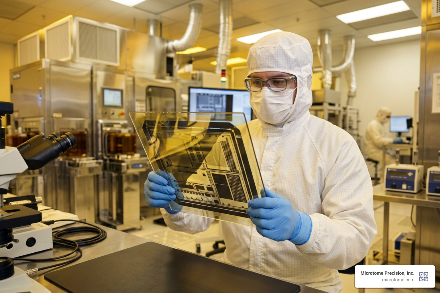
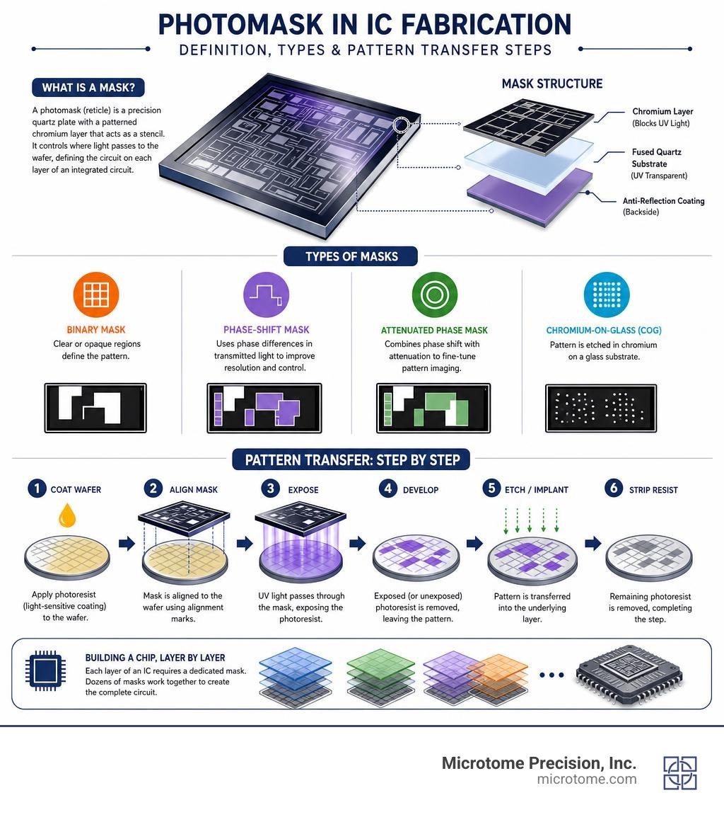
What is mask in IC fabrication? A mask (also called a photomask or reticle) is a precision plate — typically made from fused quartz with a patterned chromium coating — that acts as a stencil. It controls where light reaches the silicon wafer during photolithography, defining every transistor, interconnect, and feature on each layer of an integrated circuit.
Here is a quick summary:
| Term | What it means |
|---|---|
| Photomask / Mask | Opaque plate with transparent areas that pass light in a defined pattern |
| Reticle | Modern term for a mask used in a stepper or scanner; typically 4-5x larger than the final printed feature |
| Chromium layer | Blocks UV light where the circuit pattern should not print |
| Fused quartz substrate | Holds the pattern; chosen for low thermal expansion and UV transparency |
| Photoresist | Light-sensitive coating on the wafer that reacts to the pattern the mask projects |
| Mask set | Full collection of masks — sometimes 30 or more — needed to build all layers of one chip |
Every layer of a chip requires its own dedicated mask. The mask is exposed through an optical system that shrinks and projects the pattern onto the wafer, step by step, until the full circuit is built up.
Masks are among the most precise — and most vulnerable — objects in semiconductor manufacturing. A single high-end phase-shift mask can represent enormous value, weeks of lead time, and zero tolerance for defects. Particles, chemical contamination, and electrostatic hazards are constant threats to mask integrity.
I’m Matt Pilarski, President of Microtome Precision, Inc., where we have specialized in reticle carrier design and manufacturing since 1989 — longer than any other independent company in this field. Our work sits at the intersection of everything covered in this guide: the moment a mask leaves the mask shop and must be protected through storage, transport, and repeated use in the fab, which is precisely where understanding what is mask in IC fabrication becomes critical for yield, uptime, and cost control.
Understanding What Is Mask in IC Fabrication
To fully grasp what is mask in IC fabrication, we must look at how a photomask functions as an optical blueprint. At its core, a Photomask is a high-purity glass or quartz plate covered with an extremely thin, opaque absorbing film (usually chromium). By etching away portions of this chromium layer, we create a microscopic pattern of transparent and opaque regions.
In modern fabs, the terms “mask” and “reticle” are often used interchangeably, though they historically had distinct meanings. A traditional photomask contained a 1:1 scale pattern of the entire wafer layout and was used in contact or proximity aligners. A reticle, by contrast, contains the pattern for only a few die (or even a single die) and is designed for projection lithography systems like steppers and scanners. These systems use advanced reduction optics to project the reticle’s pattern at a 4x or 5x reduction ratio onto the wafer surface, as explained by the Mask | Samsung Semiconductor Global dictionary.
The choice of materials is highly engineered. Fused silica (quartz) is the gold standard for optical lithography because it is highly transparent to deep ultraviolet (DUV) light wavelengths (such as 193 nm) and exhibits an exceptionally low coefficient of thermal expansion. This ensures that even under the intense energy of DUV laser exposure, the mask does not warp or distort, which would otherwise ruin pattern overlay accuracy.
Historical Evolution of Mask Making
The history of mask making is a testament to the rapid scaling of Moore’s Law. In the early days of the semiconductor industry, circuit layouts were hand-drawn on giant sheets of red masking film called Rubylith. These massive artworks, which could easily fill an entire room wall, were then photographically reduced through high-precision cameras onto glass plates.
As feature sizes shrank below the limits of manual drafting, the industry transitioned to optical pattern generators. These machines used a variable rectangular aperture to expose photoresist on a mask blank plate, flashing thousands of individual rectangles to build up the circuit layout. While a major step forward, optical pattern generators eventually gave way to electron-beam (e-beam) lithography and high-speed laser writers, which are standard today.
E-beam lithography uses a highly focused beam of electrons to write nanometer-scale patterns directly into a resist layer on the mask blank. This direct-write capability is incredibly precise, though writing times are governed by pattern density and write-grid resolution rather than simple geometric complexity. For a deeper look at these early techniques, you can explore the Layout and Mask Conventions guide. To understand how these manufacturing pipelines operate in the modern era, refer to the How Photomasks for IC Production Are Made (2025 Guide).
How Photomasks Transfer Patterns to Silicon
The transfer of a pattern from a mask to a silicon wafer is accomplished through photolithography. The process begins by coating the silicon wafer with a uniform layer of a light-sensitive polymer called photoresist.
The wafer and the mask are loaded into an exposure tool (a stepper or scanner). The tool aligns the mask to existing features on the wafer with nanometer precision. Once aligned, a high-intensity UV light source shines through the mask. The light passes through the clear quartz regions but is blocked by the opaque chromium regions.
Depending on the type of photoresist applied, the chemical reaction differs:
- Positive Photoresist: The areas exposed to light become soluble in a chemical developer solution. The unexposed areas remain intact, leaving a replica of the mask’s dark features on the wafer.
- Negative Photoresist: The exposed areas undergo cross-linking, making them insoluble in the developer. The unexposed areas are washed away, leaving a replica of the mask’s clear features.
Once developed, the remaining photoresist acts as a protective barrier during subsequent etching or ion implantation steps. This process sequence is repeated dozens of times, using a different mask for each layer, to build up the entire three-dimensional integrated circuit. A visual breakdown of this entire flow can be watched in the video on Fabrication Processes of a Chip: Photolithography.
Types of Photomasks and Their Materials
Photomasks are categorized by how they manipulate light to achieve the desired resolution on the wafer. As feature sizes have shrunk far below the wavelength of the light used to print them, mask technology has evolved from simple “shadow masks” to complex optical instruments.
- Binary Masks: The traditional and simplest type of mask. They consist of a clear quartz substrate with an opaque chromium pattern. Light either passes through completely (100% transmission) or is blocked entirely (0% transmission).
- Phase-Shift Masks (PSM): These masks improve lithographic resolution by exploiting the wave nature of light. By shifting the phase of light passing through adjacent clear regions by 180 degrees, the light waves destructively interfere at the boundary. This creates a much sharper transition from light to dark on the wafer, allowing for smaller features to be printed.
- Embedded Attenuated PSMs (EAPSM): A variation where the chromium is replaced with a partially transmitting material (like molybdenum silicide, MoSi) that shifts the phase of the transmitted light by 180 degrees while attenuating its intensity to about 6%. This creates a similar phase-shifting interference effect without requiring complex quartz etching.
- EUV Masks (Extreme Ultraviolet): Because EUV light (13.5 nm wavelength) is absorbed by almost all matter, including glass and quartz, transmissive masks cannot be used. Instead, EUV masks are completely reflective. They consist of a substrate coated with a highly reflective Bragg reflector made of alternating layers of molybdenum and silicon (typically 40 to 50 bilayer pairs), topped with an absorber layer that is etched to form the pattern.
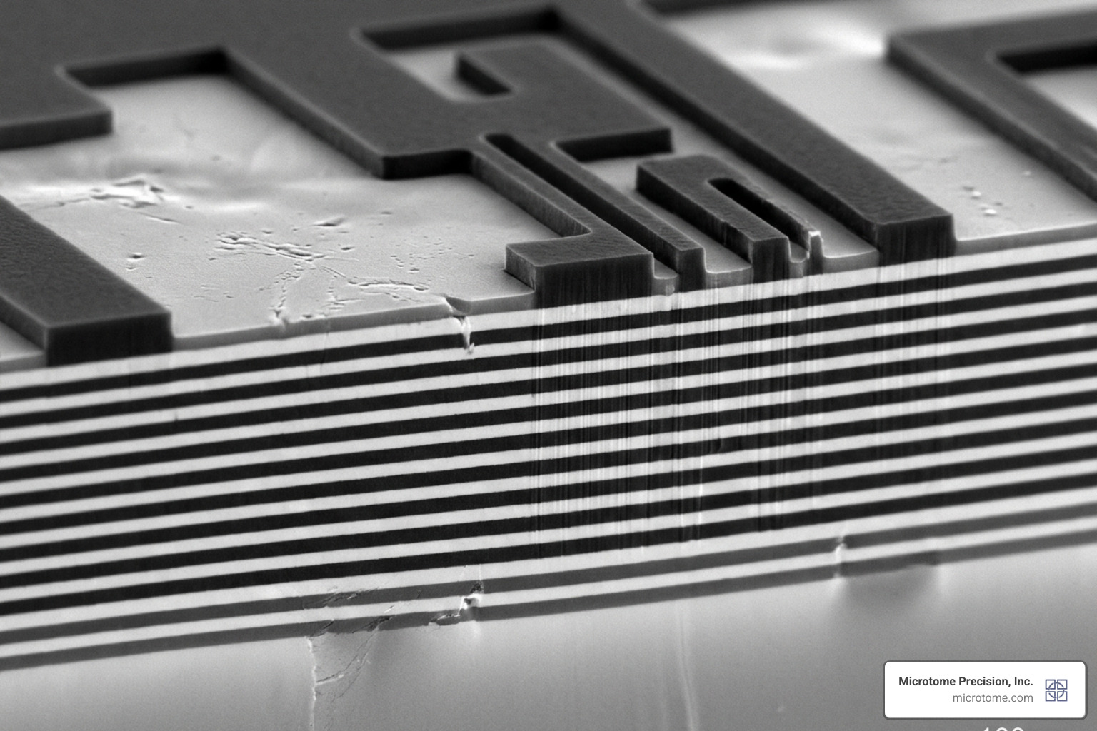
Beyond these photolithographic templates, the industry also utilizes “hard masks” on the wafer level. While photomasks are the external optical tools used to project the pattern, a hard mask is an inorganic thin film (such as silicon dioxide, silicon nitride, or metals like titanium nitride) deposited directly onto the wafer substrate. It is used when the soft photoresist layer is too thin or lacks the chemical resistance to survive deep, aggressive plasma etching. For an in-depth exploration of wafer-level hard masks, see the technical guide on Hard Mask Processing: Materials, Integration, and Pattern Transfer Strategies | NineScrolls LLC.
To understand where our products fit in, you can read more about how we support these diverse lithography technologies on our Blog.
| Mask Type | Substrate Material | Absorber/Reflector Material | Typical Lithography Nodes | Primary Optical Mechanism |
|---|---|---|---|---|
| Binary Mask | Fused Silica (Quartz) | Chromium (Cr) | Legacy to 90 nm | Simple transmission / absorption (shadowing) |
| Phase-Shift Mask (PSM) | Fused Silica (Quartz) | Molybdenum Silicide (MoSi) + Chrome | 90 nm to 7 nm (DUV) | Phase destructive interference at feature edges |
| EUV Mask | Low Thermal Expansion Material (LTEM) | Mo/Si Multilayers (Reflector) + Ta-based Absorber | Sub-7 nm (EUV) | Bragg reflection with selective absorption |
Substrate and Coating Selection
The physical performance of a photomask depends heavily on its substrate and coating materials. Fused silica remains the primary substrate for DUV lithography due to its excellent deep-UV transparency and low thermal expansion. For less critical, larger-feature legacy nodes (such as those above 1 micron), soda-lime glass is sometimes used because of its lower cost, though its high thermal expansion coefficient makes it unsuitable for sub-micron matching.
For coatings, chromium is the standard absorber because of its excellent adhesion to quartz, high optical density, and ease of dry etching. In older or specialized optical alignment systems, semi-transparent iron oxide coatings are occasionally preferred. Iron oxide blocks actinic UV exposure wavelengths while remaining semi-transparent to visible light, allowing tool operators to visually align the mask to the wafer underneath before exposure. Additional material specifications and manufacturing options can be reviewed at Photo Mask.
Mask Design, Data Prep, and Resolution Enhancement
The path from an IC designer’s schematic to a finished physical mask is incredibly complex. Once a chip design is finalized, the physical layout is exported as a massive hierarchical data file, typically in GDSII or OASIS formats.
Before this data can be sent to a mask-writing tool, it must undergo Mask Data Preparation (MDP). As detailed in the Mask data preparation workflow, MDP translates the complex, overlapping polygons of the chip layout into simplified geometric instructions (such as rectangles and trapezoids) that the mask writer’s e-beam or laser can physically execute. This polygon simplification is known as mask fracturing.
Computational Challenges in What Is Mask in IC Fabrication Design
The computational resources required for modern MDP are staggering. When feature sizes are smaller than the wavelength of the exposure light, the light diffuses and diffracts, causing nearby shapes to bleed into one another. This is known as the proximity effect.
To prevent shorts and open circuits, every single shape on every mask layer must be mathematically adjusted to compensate for these optical distortions. Correcting these proximity effects across a state-of-the-art chip layout containing billions of shapes can consume a tremendous amount of computing resources. For a single critical layer, full-chip optical correction can easily require over 440 CPU hours — equivalent to more than 18 days of dedicated, continuous computing time on a high-performance server.
To manage this computational bottleneck, design teams often pre-correct standard cell libraries or partition layouts into internal and boundary regions, minimizing the need to recalculate identical shapes. For a practical look at how these layers are organized and named at a process level, you can review the Masks — SkyWater SKY130 PDK documentation.
Resolution Enhancement Techniques
To push optical lithography far beyond its theoretical physical limits, the industry relies on Resolution Enhancement Techniques (RET). These advanced computational and optical strategies modify the mask layout so that the highly distorted light waves reconstruct themselves into the correct shape once they reach the wafer.
- Optical Proximity Correction (OPC): OPC alters the polygons on the mask to compensate for diffraction. It adds tiny “serifs” to the corners of square pads to keep them from rounding off on the wafer, and thins or widens lines to ensure uniform critical dimensions (CD).
- Sub-Resolution Assist Features (SRAF): SRAFs are extremely narrow lines placed alongside main layout features. These assist features are too small to physically print on the wafer themselves, but their presence alters the local diffraction pattern, significantly improving the depth of focus and contrast of the primary features.
- Mask Error Enhancement Factor (MEEF): As features shrink, MEEF increases. MEEF is a metric that describes how much a dimensional error on the photomask is amplified when projected onto the wafer. If MEEF is high (e.g., greater than 1), a tiny 2 nm error on the mask can result in a catastrophic defect on the wafer, necessitating extreme precision in mask metrology and inspection.
Protecting the Mask: Contamination, ESD, and EFM Challenges
Because a single photomask is used to print the exact same pattern millions of times across thousands of silicon wafers, any defect on the mask is a systemic disaster. A single particle landing on a critical mask feature will act as a permanent blocker, printing a “repeating defect” on every single wafer exposed, destroying the yield of the entire production run.
To prevent falling cleanroom particles from settling on the mask surface, fabs use pellicles. A pellicle is a thin, optically transparent membrane stretched over a metal frame and mounted directly to the mask. The pellicle stands a few millimeters above the quartz surface. Any airborne particle that falls onto the mask assembly lands on the pellicle instead of the quartz. Because the pellicle is held outside the focal plane of the exposure optics, the shadow of the particle is completely out of focus and does not print onto the wafer.
However, pellicles do not solve every contamination issue. Fabs running high-power 193 nm DUV lithography frequently encounter reticle haze. Haze is a form of crystal growth that occurs on the mask surface over time. It is triggered when deep-UV laser energy acts as a catalyst, breaking down trace chemical residues — such as ammonium ions, sulfates, and airborne molecular organics — inside the reticle environment. This chemical reaction leads to crystal nucleation and growth, which eventually scatters light and ruins the mask.
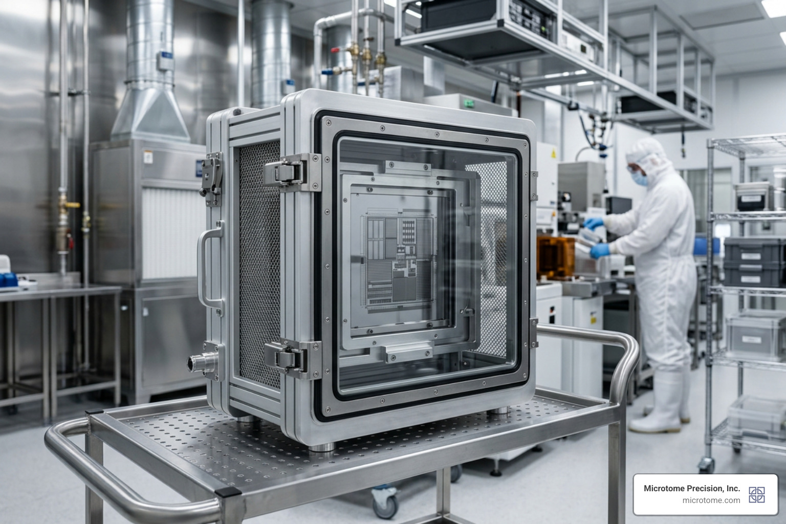
To prevent haze, masks must be stored and transported in ultra-clean reticle pods that are constantly purged with clean dry air (CDA) or nitrogen to eliminate moisture and chemical contaminants. You can read more about how our advanced carrier systems integrate with these cleanroom environments on our Compatibility page.
Safeguarding What Is Mask in IC Fabrication from Electrostatic Hazards
While physical particles and chemical haze are major yield-killers, the most insidious threat to photomask integrity is electrostatic. In the semiconductor industry, there is a common misconception that standard Electrostatic Discharge (ESD) controls are sufficient for reticle protection. This is a highly dangerous assumption.
Reticles require a fundamentally different protection paradigm than standard silicon wafers or general cleanroom equipment. While wafers are vulnerable to high-voltage ESD events, photomasks are highly sensitive to Electric Field induced Migration (EFM).
EFM is a physical phenomenon where sub-micron chrome features on a reticle degrade, peel, or migrate under the influence of relatively weak, localized electrostatic fields. This damage occurs at voltage thresholds far below what would trigger a classic spark or ESD event. An external electric field — generated by charged cleanroom plastics, human operators, or robotic handlers — can polarize the isolated chrome lines on the reticle, creating localized field stresses that attract airborne molecular contaminants and sub-micron particles directly to the active clear areas of the mask.
To make matters worse, conventional ESD countermeasures can actually increase the risk of EFM on reticles:
- Static-Dissipative and “Conductive” Plastics: Many standard reticle pods are made from static-dissipative plastics. While these materials prevent rapid ESD sparks, they do not block external electric fields. In fact, they allow slow charge accumulation and field penetration, which can actively drive EFM on the enclosed reticle.
- Air Ionizers: While useful for neutralizing surface charges on large, open workbenches, air ionizers do not provide instantaneous protection inside closed storage environments and can sometimes introduce highly charged air currents into the cleanroom.
The only way to completely protect a reticle from EFM is to isolate it within a perfect Faraday cage. An all-metal, conductive enclosure blocks all external electric fields, ensuring that the electric potential inside the carrier remains completely uniform and zero field stress is applied to the reticle.
At Microtome Precision, we design and manufacture all-metal Faraday-cage reticle carriers that meet and exceed SEMI E111 (specifications for single reticle pods) and SEMI E112 (specifications for multi-reticle cassettes) standards. By eliminating the use of static-dissipative plastics in our structural shells, we provide absolute EFM protection, safeguarding your high-value Photomask assets from invisible electrostatic degradation.
Frequently Asked Questions about Photomasks
What is the difference between a photomask and a reticle?
In modern semiconductor manufacturing, “photomask” and “reticle” are often used as synonyms, but they have a distinct historical difference based on the lithography system’s optical layout:
- Photomask: Historically referred to a 1:1 scale plate that matched the entire wafer area. It was clamped directly against or held just above the wafer in contact or proximity aligners.
- Reticle: Refers to a plate that contains only a portion of the wafer’s pattern (such as a single die or a small cluster of die). It is designed for projection lithography (steppers and scanners), where the light is passed through reduction optics. This projects the pattern onto the wafer at a reduced scale, typically 4x or 5x smaller than the physical features on the reticle itself. Because modern manufacturing exclusively uses reduction projection tools, almost all modern masks are technically reticles.
Why are EUV masks reflective instead of transmissive?
EUV lithography utilizes an extremely short wavelength of light (13.5 nm) to print sub-7 nm features. At this wavelength, extreme ultraviolet light is highly absorbed by virtually all physical materials, including the high-purity fused silica glass used for standard DUV photomasks. Because no suitable transmissive substrate material exists for EUV, the entire optical system must be reflective.
An EUV mask acts as a mirror rather than a stencil. It is built on a specialized substrate with ultra-low thermal expansion, coated with a reflective Bragg reflector consisting of 40 to 50 alternating nanometer-scale layers of molybdenum and silicon. The circuit pattern is then etched into an absorbing layer deposited on top of this reflective stack. Where the absorber is removed, EUV light reflects off the Mo/Si mirror and into the projection optics; where the absorber remains, the light is blocked.
How does EFM damage a photomask or reticle?
Electric Field induced Migration (EFM) is an electrostatic degradation process unique to sub-micron patterned photomasks. When a reticle is exposed to an external electrostatic field (even a weak one), the isolated chromium lines on the quartz substrate become polarized. This polarization creates intense, localized electric field gradients at the edges of the chrome features.
These localized fields act as electrostatic magnets, attracting polar molecules, airborne molecular contaminants (AMCs), and charged sub-micron particles directly out of the surrounding air. Over time, these attracted contaminants deposit onto the edges of the chrome features, causing localized “haze” growth, line-edge roughness, and eventual dimensional changes. In severe cases, the electrostatic field stress can cause the thin chrome lines to physically delaminate or migrate across the quartz substrate, permanently destroying the reticle’s pattern and leading to repeating lithographic defects on the silicon wafers.
Conclusion
Understanding what is mask in IC fabrication is essential for anyone involved in modern semiconductor manufacturing. From the complex computational math of mask data preparation to the delicate physics of phase-shift and EUV lithography, the photomask is the ultimate physical gatekeeper of chip yield and performance.
Because photomasks are highly sensitive to microscopic contamination, reticle haze, and electrostatic hazards, protecting them is a critical operational priority. Since 1989, we at Microtome Precision, Inc., based in Colorado Springs, Colorado, USA, have dedicated our business to this exact mission. As the longest-established independent manufacturer of reticle carriers, we specialize in designing and building SEMI E111 and E112 compliant all-metal SMIF pods and cassettes. Our proprietary Faraday-cage designs provide absolute protection against EFM and cleanroom contamination, ensuring your mask sets perform flawlessly from first exposure to last.
To learn more about our Faraday-cage reticle carriers, explore our Products Overview. If you have existing carriers that require servicing, we also offer a comprehensive Support and Repair program to recertify your equipment to original factory specifications. Let us help you protect your lithography yield.