How to Clean Reticle: 5 Simple Steps
Why Reticle Cleaning Determines Semiconductor Yield
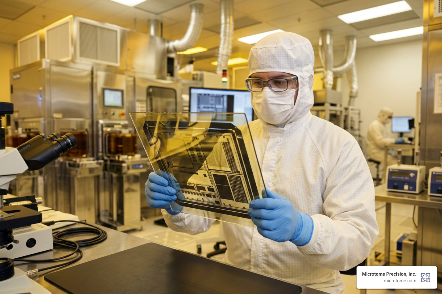
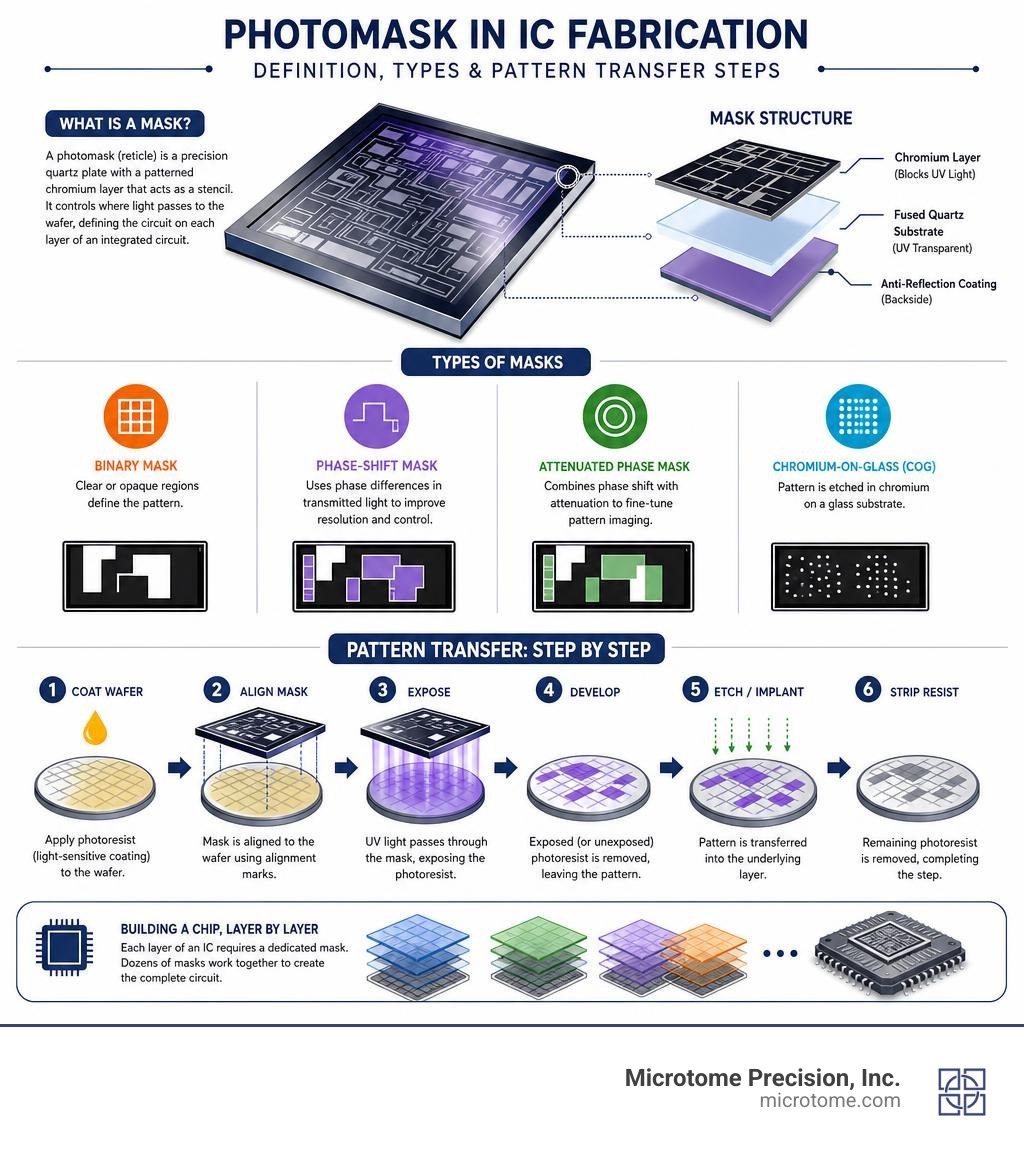
Reticle cleaning is the process of removing particles, organic residues, and thin films from a semiconductor photomask — the master template used to project circuit patterns onto silicon wafers during lithography.
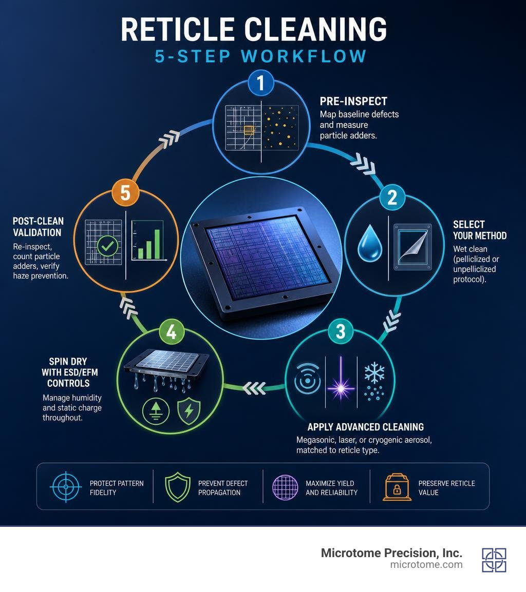
Quick answer: How to clean a reticle in 5 steps
- Pre-inspect — map baseline defects and measure particle adders before cleaning
- Select your method — wet clean (pelliclized or unpelliclized protocol)
- Apply advanced cleaning — megasonic, laser, or cryogenic aerosol, matched to reticle type
- Spin dry with ESD/EFM controls — manage humidity and static charge throughout
- Post-clean validation — re-inspect, count particle adders, verify haze prevention
A single reticle is used to expose every die on every wafer in a production run. That means one particle, one organic residue, or one contaminating film on the mask surface can print a defect across thousands of chips. The consequences are not limited to scrap — they can propagate through an entire lot before anyone detects the source.
Contamination on a reticle is also not always obvious. Defects at the edges of pattern features are harder to detect and carry a higher mask error enhancement factor (MEEF), making them more likely to print and more damaging to yield than defects in open areas. Over-cleaning creates its own risk: repeated wet cleaning cycles can erode the mask pattern itself, shifting critical dimension uniformity (CDU) in ways that affect device performance.
This is why reticle cleaning is not a simple maintenance task. It requires validated protocols, calibrated equipment, and contamination controls that extend well beyond the cleaning step itself — including how the reticle is stored, transported, and protected between cleaning cycles.
I’m Matt Pilarski, President of Microtome Precision, Inc., where we have specialized in reticle carrier design and photomask contamination control since 1989 — including Microtome’s 2003 discovery of EFM (Electric Field induced Migration), a reticle failure mode that standard ESD controls do not address and can actually worsen. The reticle cleaning guidance below draws on that decades-long focus on protecting high-value photomasks at every stage of their lifecycle.
The Science of Reticle Cleaning in Advanced Lithography
In advanced deep ultraviolet (DUV) and extreme ultraviolet (EUV) lithography, the physical limits of contamination control are pushed to the atomic scale. At these sub-10nm nodes, even a single particle measuring a mere 20 nanometers can cause catastrophic pattern transfer failures. Understanding the physical and chemical interactions on the photomask surface is essential to designing an effective cleaning strategy.
The primary metric for evaluating any cleaning process is “particle adders per clean cycle.” A particle adder is any contaminant deposited on the reticle surface during the cleaning, handling, or drying process itself. Ideally, a cleaning cycle should have a negative adder count—meaning it removes existing contaminants without introducing new ones.
To validate a clean cycle, engineers use high-resolution inspection tools to map the reticle before and after processing. This validation is critical because DUV and EUV exposure tools use highly energetic light (193 nm for DUV and 13.5 nm for EUV) that acts as a catalyst. When this light hits trace organic residues or moisture on the reticle, it triggers chemical reactions that lead to crystal growth, commonly known as “reticle haze.”
Furthermore, any defect on the pattern edges alters the wavefront of the light passing through or reflecting off the reticle. Because of the Mask Error Enhancement Factor (MEEF), a tiny defect on the reticle can translate into a significantly larger defect on the wafer. This directly degrades Critical Dimension Uniformity (CDU), leading to localized timing errors or complete circuit failures on the microchip.
While basic consumer optics cleaning guides (such as How to Clean a Rifle Scope and Optics – Accufire , Cleaning optics…Tutorial | Rimfire Central Firearm Forum , or PRECISION COATED OPTICAL Lenses, Corrector Plates and other ) rely on manual wiping and simple solvents, semiconductor photomasks require automated, damage-free molecular removal. Advanced tools like those discussed in Reticle Wet Cleaning – Nanomaster Europe utilize non-contact chemical and physical forces to clean without degrading the delicate absorber patterns.
Our team regularly discusses these complex yield-limiting mechanisms on the Microtome Precision Blog, highlighting how pre-clean and post-clean handling environments dictate overall mask longevity.
5 Steps to Clean and Validate a Semiconductor Reticle
Achieving a zero-particle-adder cleaning cycle requires a highly disciplined, multi-step process executed within a Class 1 (ISO 3) or cleaner environment. Every step must be tightly controlled to prevent mechanical damage, chemical erosion, or electrostatic discharge.

Step 1: Pre-Inspection and Particle Adder Measurement
Before any chemical or physical cleaning agent touches the reticle, you must establish a baseline.
- STARlight Methodology: Most modern mask shops and fabs utilize database-free inspection technologies like STARlight. This methodology compares transmitted and reflected light images taken simultaneously across the reticle. Because it does not require access to the original CAD database, it can quickly identify localized defects, contaminating films, and edge-of-pattern variations directly in the fab.
- Defect Mapping: The inspection system generates a high-resolution spatial map of all pre-existing defects, categorizing them by size, coordinates, and optical properties (reflectivity and transmissivity).
- Particle Size Categorization: Particles are binned into specific size ranges (e.g., <20nm, 20-50nm, >50nm). This categorization helps determine the aggressive nature of the cleaning recipe required. If only large, loose particles are present, a gentle megasonic rinse may suffice, avoiding the pattern-eroding risks of harsh acids.
Step 2: Selecting the Wet Reticle Cleaning Method (Pelliclized vs. Unpelliclized)
The presence of a pellicle — a thin, transparent membrane mounted above the reticle surface to keep falling particles out of the focal plane — dictates your entire cleaning chemistry and physical handling strategy.
- Pelliclized Masks: Cleaning a pelliclized reticle is exceptionally challenging because you must avoid direct contact with the delicate pellicle membrane. The process focuses on cleaning the backside of the quartz substrate and the front-side alignment marks outside the pellicle frame. Specialized systems use localized megasonic DI water nozzles and protective physical cups to shield the pellicle from chemical seepage or condensation.
- Unpelliclized Masks: Unpelliclized reticles, or those prepared for re-pelliclization, allow full-surface exposure to wet chemistries. This includes removing the old frame adhesive from the mounting borders.
- Chemical Formulations:
- Acidic Chemistries: Sulfuric acid and hydrogen peroxide mixtures (SPM) are highly effective at stripping organic residues, but they risk eroding delicate transition-metal absorber layers.
- Basic Chemistries: Ammonium hydroxide and hydrogen peroxide mixtures (APM) help remove particles by generating electrostatic repulsion between the particles and the reticle surface, though they must be carefully timed to prevent quartz etching.
- Neutral/Ozonated Chemistries: Ozonated deionized water ($O3/DIW$, typically at 20 ppm of $O3$) is increasingly favored as a highly effective, environmentally friendly alternative that minimizes pattern erosion.
For systems designed to handle both variations, platforms like those detailed in Pelliclized and Unpelliclized Reticle Cleaning Systems – Nano-Master (also referenced as Pelliclized and Unpelliclized Reticle Cleaning Systems) provide configured dual-dispense paths to isolate chemistry based on the mask configuration.
Step 3: Applying Advanced Reticle Cleaning Technologies
Once the appropriate chemical environment is established, physical force is applied to overcome the boundary layer and detach sub-micron particles from the reticle surface.
- Megasonic Cleaning: This is the industry standard for non-contact particle removal. High-frequency acoustic waves (typically 800 kHz to 1.5 MHz) are transmitted through the cleaning liquid. This creates micro-cavitation and acoustic streaming. The energy must be tightly controlled below the “damage threshold” of the sub-100nm chromium, molybdenum silicide (MoSi), or EUV ruthenium absorber lines to prevent pattern peeling.
- Laser-Based Cleaning: Short-pulse lasers (nanosecond or femtosecond) can be targeted at stubborn, localized particles. The rapid thermal expansion of the particle or a thin, pre-applied liquid film under the laser shot ejects the contaminant without heating the underlying quartz.
- Cryogenic Aerosol Cleaning: This dry technique uses pressurized liquid carbon dioxide ($CO2$) or argon/nitrogen mixtures expanded through a nozzle to form solid micro-snow particles. Upon striking the reticle surface, these cryogenic particles transfer momentum to contaminants, freezing and lifting them. The $CO2$ then sublimates directly back into gas, leaving zero liquid residue or watermarks.
Step 4: Controlled Spin Drying and ESD/EFM Prevention
The drying phase is historically the highest-risk step for both watermark formation and electrostatic damage. As water is flung off a rotating reticle, friction between the liquid and the dielectric quartz substrate generates massive triboelectric charges.
- The Risk of Triboelectric Charging: If these charges are allowed to accumulate, they build up intense electric fields across the microscopic gaps of the reticle pattern.
- ESD vs. EFM: While a sudden, high-voltage Electrostatic Discharge (ESD) can melt or vaporize pattern lines, a far more insidious phenomenon occurs at much lower voltage levels: Electric Field induced Migration (EFM). EFM causes metal atoms (especially chrome or molybdenum) to slowly migrate across the quartz substrate when exposed to an electric field. Over time, this alters the pattern geometry, degrades transmission, and destroys reticle calibration.
- The Failure of Conventional ESD Controls: Many fabs attempt to mitigate this during cleaning using air ionizers, static-dissipative plastics, or grounding straps. However, active air ionization can actually introduce unbalanced ions that worsen localized electric fields on isolated reticle structures. Furthermore, static-dissipative or “conductive” polymers do not provide true electrostatic shielding; they merely slow down charge transfer, which is entirely inadequate for preventing EFM.
- Active Neutralization Patent: Advanced systems, such as the one described in the Reticle cleaning system and method for using the same – Patent Application , address this by integrating real-time static charge sensors with active neutralization. This includes maintaining relative humidity inside the spin chamber at or above 45% RH (which provides a thin, natural moisture layer to safely dissipate charge) and using grounded conductive frames in direct contact with the reticle edges.
Step 5: Post-Clean Validation and Haze Prevention
The cleaned and dried reticle must be validated before it is cleared to return to the lithography bay.
- Post-Inspection and Adder Counting: The reticle is run through the STARlight or die-to-database inspection tool a second time. The post-clean defect map is mathematically compared to the pre-clean map. The net difference determines the exact number of “adders.”
- Haze Prevention and Purging: To ensure that trace chemical residues do not react under the DUV/EUV laser to form ammonium sulfate or carbonate haze, the validated reticle must be immediately isolated. The reticle is placed into a specialized carrier and continuously purged with Extreme Clean Dry Air (XCDA) or high-purity Nitrogen ($N_2$) to eliminate moisture and airborne molecular contamination (AMC).
| Cleaning Parameter | Wet Cleaning (Megasonic/Chemical) | Dry Cleaning (Cryogenic/Laser) |
|---|---|---|
| Primary Mechanism | Chemical dissolution & acoustic boundary layer reduction | Momentum transfer (impact) & thermal shock ejection |
| Pattern Damage Risk | Low to Moderate (depends on megasonic power & chemical pH) | Low (when laser fluence & aerosol pressure are calibrated) |
| Watermark Risk | Moderate to High (requires precise spin-dry/Marangoni dry) | Zero (completely dry sublimation) |
| ESD/EFM Risk | High (triboelectric charging during high-speed spin dry) | Low (minimal liquid friction, but gas flow can charge) |
| Adhesive Removal | Excellent (dissolves frame adhesives easily) | Poor (cannot effectively strip polymer adhesives) |
Automated Equipment and Innovations in Reticle Cleaning
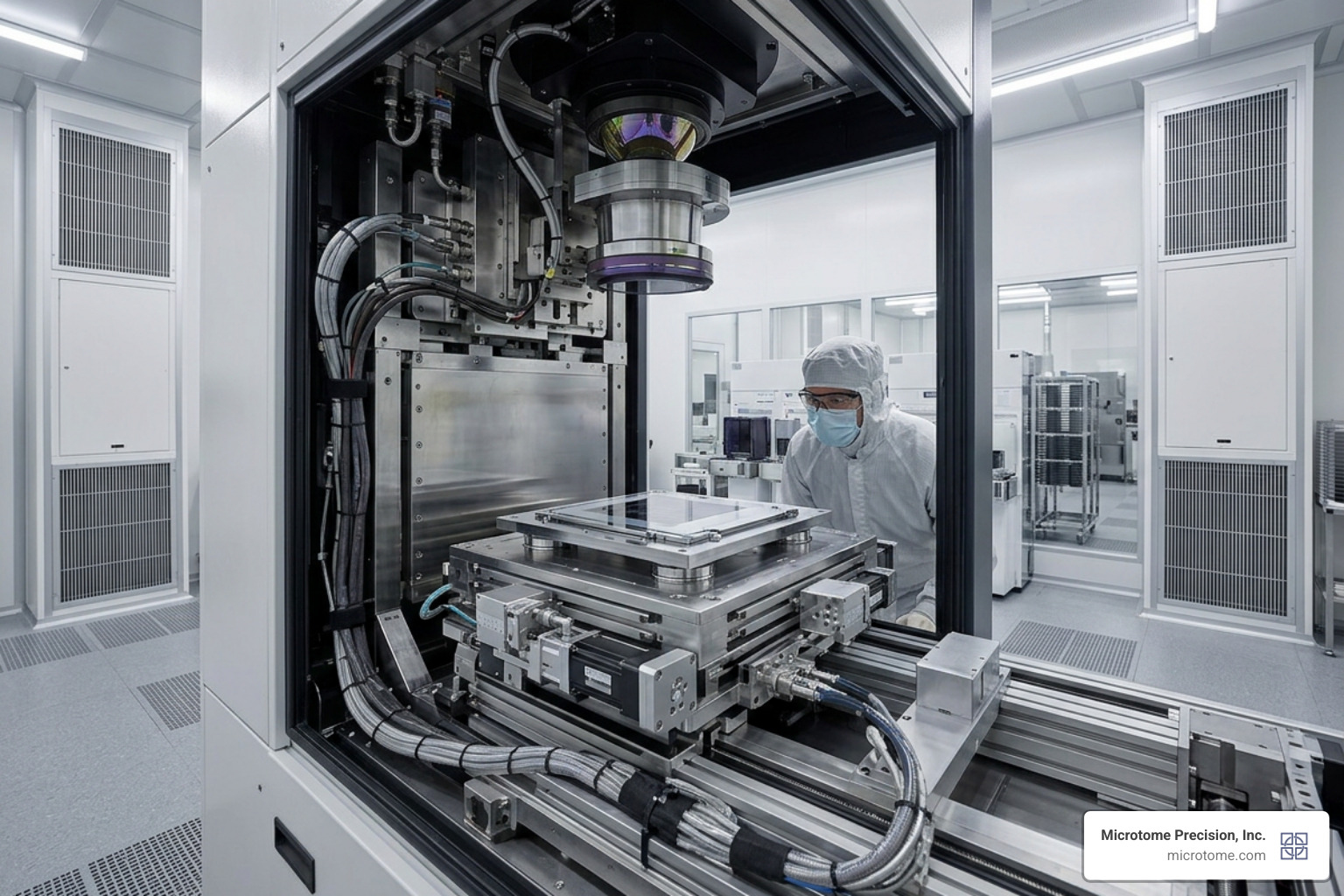
As semiconductor feature sizes shrink, manual handling of photomasks has been completely phased out in commercial production. Automated systems ensure that every step of the cleaning process is perfectly repeatable and isolated from human contamination.
Just as specialized industrial cleaning services in Colorado Springs—ranging from heavy machinery restoration at DPF Alternatives Colorado Springs, CO and Colorado to precision firearms maintenance at Gun Cleaning Services Colorado and biohazard remediation at “Home – NextStep Colorado Springs Crime Scene Cleaning” —require highly specialized, regulated equipment, semiconductor photomask maintenance requires cleanroom-grade automated systems.
Key Features of Automated Reticle Cleaning Systems
Modern automated platforms, such as the NANO-MASTER LSC-5000, are built to process advanced masks with extreme precision. These systems typically feature:
- Robotic Loading and EFEM/SMIF Interface: Reticles are loaded directly from SMIF pods or cassettes using robotic arms equipped with vacuum or edge-grip end effectors. This prevents any physical contact with the active patterned area.
- Dual Dispense Arms: Separate, independently controlled arms apply chemicals and DI water. This design prevents cross-contamination between acidic strip solutions, basic particle-removal chemistries, and neutral rinses.
- Environmental Chambers: The entire cleaning and drying process takes place within a sealed, positive-pressure chamber. This chamber features integrated HEPA/ULPA filtration, active relative humidity control (typically locked above 45% RH to suppress static generation), and real-time exhaust monitoring.
AI and Machine Learning in Reticle Cleaning Optimization
The latest evolution in automated reticle cleaning is the integration of AI and machine learning algorithms to optimize process recipes.
Instead of relying on rigid, time-based cleaning cycles, AI-driven systems analyze historical defect maps and particle adder trends across hundreds of cleaning runs. If the system detects a recurring pattern of 30nm particles after processing a specific reticle type, it automatically adjusts the megasonic transducer’s power output, alters the chemical dispense dwell time, or modifies the spin-dry ramp speed.
This adaptive cleaning approach minimizes pattern erosion by ensuring the reticle is never exposed to more chemical or physical force than is absolutely necessary to remove the mapped contaminants. Fabs can verify equipment compatibility and integrate these automated recipes across their legacy and next-generation lithography tools by consulting our Compatibility matrix.
Frequently Asked Questions about Photomask Maintenance
What are particle adders and how are they measured?
Particle adders are contaminants deposited on a reticle during a process cycle (such as cleaning, handling, or transport). They are measured by running a high-resolution optical inspection (like STARlight) before and after the cycle, then mathematically subtracting the initial defect map from the final map to determine the net quantity and size of the new particles.
How does cleaning differ for pelliclized vs. unpelliclized reticles?
Unpelliclized reticles allow full-surface exposure to wet chemicals, megasonic agitation, and spin drying across both the front and back sides. Pelliclized reticles cannot be directly touched or exposed to open liquids on the front patterned surface; instead, automated systems use localized nozzles to clean the backside and alignment marks while protecting the pellicle membrane from chemical exposure, condensation, or pressure differentials.
How do environmental conditions affect electrostatic risk during cleaning?
Low relative humidity (below 45% RH) dramatically increases the risk of triboelectric charge accumulation on the quartz substrate, especially during high-speed spin drying. This static charge creates intense electric fields that cause Electric Field induced Migration (EFM), pulling microscopic metal atoms across the quartz and permanently damaging the reticle pattern.
The Ultimate Protection Post-Clean: Complete Faraday-Cage Shielding
Once a reticle has been meticulously cleaned, dried, and validated, the battle against contamination and electrostatic damage is only half won. The moment that photomask leaves the clean chamber of the automated washing system, it is exposed to the hazards of transport, storage, and handling within the fab.
Many semiconductor facilities make the mistake of storing their freshly cleaned reticles in standard plastic SMIF pods or cassettes. While these polymers are often marketed as “static-dissipative” or “ESD-safe,” they do not block electric fields. In fact, as these plastic pods move through the fab, friction with automated guided vehicles (AGVs) or cleanroom air currents generates electrostatic fields. These fields pass directly through the plastic walls, inducing Electric Field induced Migration (EFM) on the reticle inside.
At Microtome Precision, Inc., based in Colorado Springs, Colorado, we have spent nearly four decades perfecting reticle protection. Our USP is simple: we design and manufacture all-metal, SEMI E111 and E112 compliant single-reticle pods and multi-reticle cassettes.
Because our carriers are constructed entirely of precision-machined aluminum, they act as perfect physical Faraday cages. Electric fields cannot penetrate the metal barrier; instead, any external charge is safely routed around the exterior of the pod, keeping the reticle inside in a state of absolute electrostatic rest. This completely eliminates the risk of EFM—a level of protection that no plastic carrier can ever provide.
Furthermore, our pods feature robust sealing and purge ports compatible with continuous XCDA and nitrogen systems, ensuring that clean, dry, haze-free conditions are maintained from the moment the reticle is loaded until it is placed on the exposure stage.
Protect your yield and extend the lifespan of your high-value photomasks. Explore our full range of semiconductor carriers on our Products page, or learn more about our professional maintenance options through our Support and Repair services and our Support and Repair Product Overview. Ready to upgrade your contamination control? Contact us today to discuss your fab’s specific requirements.