
Ultimate Checklist for Reticle Fab Equipment
Why Reticle Fab Equipment Is the Foundation of Semiconductor Yield
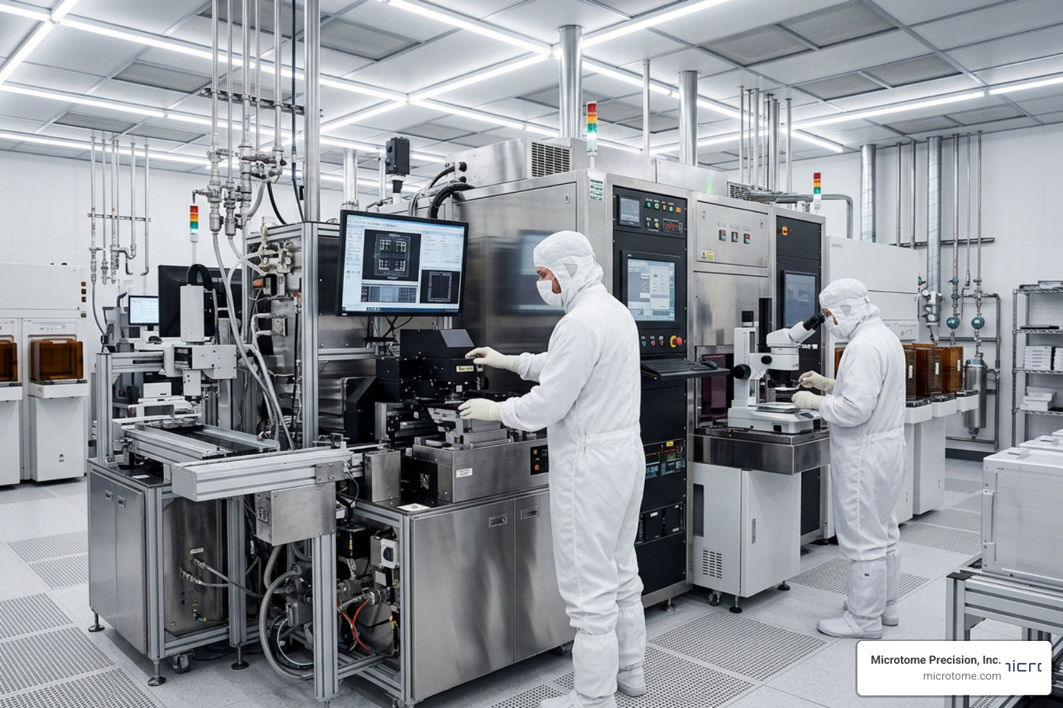
Reticle fab equipment sits at the most critical — and most expensive — point in semiconductor manufacturing: photolithography.
Every chip pattern starts as a reticle (also called a photomask). Any defect, particle, or electrostatic event on that reticle gets printed onto wafer after wafer, across thousands of die, before anyone catches it. One contaminated reticle can quietly destroy an entire production run.
Here is a quick overview of the main categories of reticle fab equipment you need to evaluate:
| Category | What It Does | Examples |
|---|---|---|
| Reticle Inspection Systems | Detects defects on finished masks before and during production use | KLA Teron, Lasertec systems |
| Reticle Metrology Systems | Measures pattern placement accuracy and overlay error | KLA LMS IPRO, X5.x |
| Pattern Writing Systems | Creates the original mask pattern | E-beam writers, laser mask writers |
| Automated Stockers | Stores reticles in clean, purged, controlled environments | Linear stockers, pod stockers |
| Transport and Handling | Moves reticles safely through the fab | AMRs, OHT, SMIF interfaces |
| Reticle Carriers and Pods | Protects reticles from contamination, particles, and electrostatic damage | All-metal pods, SMIF pods, cassettes |
| Reticle Management Software | Tracks reticle location, usage, and lifecycle across the fab | MES-integrated systems, RFID traceability |
The stakes are high. Reticles for leading-edge nodes can cost over a million dollars and take weeks to qualify. A single fab may store up to 50,000 reticles across decentralized locations — each one requiring precise timing, contamination-free handling, and full traceability across up to 50 exposure layers per product.
And yet, reticle protection — especially electrostatic protection — remains an under-invested area in many fabs.
I’m Matt Pilarski, President of Microtome Precision, Inc., the longest-established independent designer and manufacturer of reticle carriers in the semiconductor industry, with hands-on expertise in reticle fab equipment protection going back to 1989, including the discovery and characterization of EFM (Electric Field induced Migration) in 2003. This guide covers everything a fab or mask shop manager needs to evaluate, specify, and protect the full stack of reticle fab equipment.
Core Categories of Reticle Fab Equipment

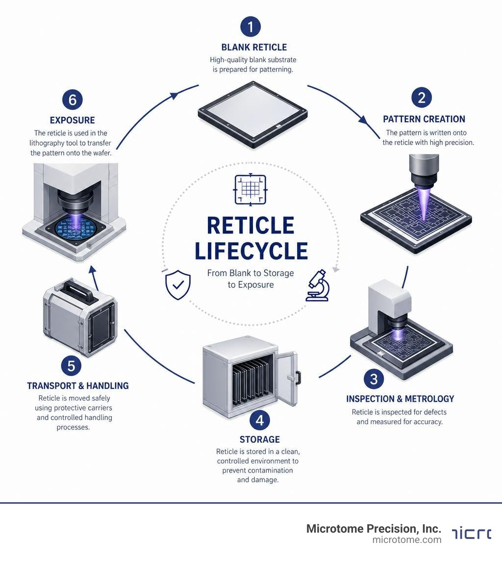
To build a world-class photolithography line, you have to look at the entire lifecycle of a reticle. The equipment required spans from the initial mask writing shop to the high-volume production floor where reticles are repeatedly inspected, measured, stored, and loaded into exposure tools.
To help clarify the division of labor in the fab, let’s contrast the two primary forms of analytical reticle fab equipment:
| Feature | Reticle Inspection Equipment | Reticle Metrology Equipment |
|---|---|---|
| Primary Goal | Detect physical defects, particles, haze, and pattern anomalies. | Measure absolute pattern placement, registration, and overlay error. |
| Typical Methods | Die-to-die, die-to-database, optical high-resolution scanning, EUV actinic light. | Laser interferometry, model-based registration algorithms, temperature-controlled stages. |
| Operational Trigger | Run before/after exposure cycles, after cleaning, and during incoming quality control. | Run during e-beam writer qualification and mask manufacturing verification. |
| Critical Metric | Defect size sensitivity (e.g., sub-2nm node detection capabilities). | Measurement precision and 3-sigma overlay accuracy (often $le$ 5 nm). |
Reticle Inspection and Metrology Equipment for Defect Detection
Because any dust, particle, or chemical residue on a mask acts as a printing defect, inspection is the primary line of defense for yield protection. In modern fabs, inspection systems operate in several modes:
- Die-to-Die (D2D) Inspection: Compares adjacent identical dies on a multi-die reticle.
- Die-to-Database (D2D) Inspection: Compares the physical reticle pattern directly against the original GDSII or OASIS design database. This is critical for complex Optical Proximity Correction (OPC) structures where minor deviations can ruin wafer yield.
For leading-edge nodes (7nm down to 2nm), Extreme Ultraviolet (EUV) lithography requires specialized actinic or high-resolution optical inspection. Systems like the KLA Teron™ 6xx series and Lasertec tools utilize advanced deep ultraviolet (DUV) and EUV wavelengths alongside specialized software to identify yield-critical defects. In particular, technologies like EUVGold and EUVMultiDie allow mask shops and fabs to qualify reticles before they ever touch a production wafer.
Metrology equipment, on the other hand, ensures that the patterns written on the reticle are exactly where they are supposed to be. Registration metrology tools like the LMS IPRO series use highly stable, temperature-controlled stages to verify pattern placement down to sub-nanometer precision. If pattern placement shifts even slightly, it contributes directly to device overlay errors in the IC fab.
To explore how these inspection environments interface with secure physical transport, view our Products Overview.
Pattern Writing and Lithography Systems
Before a reticle can be inspected or used, it must be written. Mask writing systems are highly specialized, capital-intensive tools that fall into two main categories:
- Electron-Beam (E-Beam) Lithography Systems: E-beam writers offer the highest resolution, making them the standard for writing advanced optical and EUV masks. For example, systems like the EBPG | RAITH series utilize 100 kV column technology, low-noise electronics, and high beam currents (up to 350 nA) to achieve sub-5 nm resolution with a laser interferometer resolution of 0.15 nm. E-beam writing is highly precise but slower, often requiring extreme temperature stability (such as monitoring with a MaskTemp™ system) over 24-hour write cycles.
- Laser Mask Writers: These systems use DUV lasers to write non-critical mask layers much faster than e-beam writers. They are ideal for mature technology nodes where feature sizes are larger.
Once written, qualified, and delivered to the fab, reticles are loaded into lithography steppers or scanners. For instance, the Canon Stepper Reticle Guide details how a 5x reduction stepper (like the Canon FPA-3000 EX4 KrF stepper operating at 248 nm) projects the reticle pattern onto the wafer. Designers must carefully place alignment marks like TV Pre-Alignment (TVPA) marks and high-magnification multimarks on the reticle scribe lines to ensure the stepper can align successive layers with sub-micron precision.
Automated Reticle Logistics and Storage Solutions

With advanced fabs handling tens of thousands of active reticles, manual transport is a massive risk. Dropping a million-dollar EUV reticle is a nightmare scenario, but the more common killer is micro-contamination: human operators shedding particles, causing vibration, or exposing the reticle to environmental fluctuations.
Modern fabs solve this through Automated Reticle Logistics for Semiconductor Fabs solutions, which combine high-density storage with robotic transport to isolate reticles from human contact.
High-Density Stockers and Purge Systems
Reticle stockers are the central hubs of fab-wide reticle logistics. A modern linear stocker can hold up to 3,000 Reticle SMIF Pods (RSPs) in a highly space-efficient footprint.
The primary job of a stocker is not just physical storage; it is environmental preservation. Reticles are highly susceptible to “haze” — a progressive defect where chemical residues on the mask react with laser light during exposure, forming crystals that eventually print as defects.
To prevent haze, stockers like the Brooks GuardianPro™ series utilize advanced nitrogen ($N_2$) or clean dry air (CDA) purge systems. These stockers feature localized “Tec-Cell” storage slots that continuously purge individual reticle pods. This continuous purge keeps relative humidity extremely low and prevents chemical outgassing from settling on the quartz or glass substrate.
Furthermore, advanced Reticle processing system | TREA patents highlight how physical carrier components must be engineered to prevent particle generation during pedestal rotation and vacuum handling, using specialized resting pins to maintain reticle parallelism within 0.2 degrees of tilt.
Autonomous Mobile Robots and Transport Interfaces
To move reticles from storage stockers to lithography tools, fabs rely on automated material handling systems (AMHS). This includes:
- Overhead Hoist Transport (OHT): Automated tracks on the cleanroom ceiling that pick up and drop off reticle pods directly at tool load ports.
- Autonomous Mobile Robots (AMRs): Mobile robots like the HERO Scout that navigate the fab floor, transferring reticle pods between decentralized stockers and exposure tools.
These automated handlers rely on standardized mechanical interfaces (such as SMIF and 300mm load ports) to transfer reticle carriers without exposing the internal environment to cleanroom air. Ensuring that your carriers are physically compatible with these robotic interfaces is critical for seamless fab operation. You can verify tool and interface alignment on our Compatibility page.
Software Integration and Yield Protection
Even the best hardware is useless if the fab loses track of which reticle is where. A mix-up — loading the wrong reticle revision into a scanner — can result in scraping millions of dollars of wafers. Fabs require a closed-loop digital tracking system to manage reticle lifecycles.
To learn more about the operational costs of tracking failures, read our latest insights on the Blog.
Reticle Management Software and MES Integration
Reticle management software (such as camLine’s iCADA RTCL) acts as the brain of your reticle logistics. It integrates directly with the fab’s Manufacturing Execution System (MES) and automated stocker control systems.
This integration enables several key capabilities:
- Real-Time Tracking & RFID Traceability: Every reticle carrier is equipped with an RFID tag or barcode. Automated readers at every stocker, AMR, and load port update the MES in real time, completely eliminating manual mix-ups.
- Lifecycle and Maintenance Monitoring: The software tracks the exact exposure count and clean cycles of each reticle. Once a reticle reaches a predefined threshold, the system automatically routes it to inspection or cleaning rather than the lithography tool.
- Production Forecasting: Ensures the exact reticle required for a specific wafer lot is pre-retrieved from the stocker and delivered to the scanner buffer just-in-time, maximizing lithography tool utilization.
Advanced AI-Driven Defect Classification
In high-volume manufacturing, manual defect classification is a major bottleneck. When an inspection tool like a Teron system finds a potential defect, advanced software solutions use deep learning AI algorithms (such as KLA’s second-generation X30 algorithm) to classify the defect in real time.
This AI-driven automated defect classification (ADC) distinguishes between harmless surface particles (which can be cleaned) and yield-limiting pattern errors (which require mask repair or retirement). By predicting which defects are likely to print on the wafer, these systems mitigate yield risk without causing unnecessary production downtime.
Key Challenges and Standards in Reticle Handling
Despite the massive investments in multi-million dollar reticle fab equipment, many fabs continue to experience mysterious yield drops. The culprit is almost always a failure in the most basic element of the handling loop: the reticle carrier itself.
Electrostatic and Contamination Protection in Reticle Fab Equipment
While physical particles are an obvious threat, the invisible killer of reticles is electrostatic charge.
When a plastic reticle carrier moves through a cleanroom, friction generates static electricity. This electrostatic charge creates two catastrophic issues:
- Electrostatic Attraction (ESA): The charged carrier acts as a magnet, pulling microscopic airborne particles directly onto the reticle surface.
- Electric Field induced Migration (EFM): Discovered and characterized by our team in 2003, EFM occurs when strong electric fields cause metal ions (such as chrome or molybdenum silicide) on the reticle pattern to migrate, permanently distorting the reticle geometry and ruining the mask.
To combat this, we design and manufacture all-metal reticle pods that act as a perfect Faraday cage. This design completely shields the sensitive reticle inside from external electric fields, preventing both EFM and electrostatic particle attraction. Fabs looking to eliminate these invisible yield killers can learn more through our Electrostatic Protection Consultancy Service.
Carrier Design and Material Selection
Standard plastic SMIF pods are prone to outgassing, static accumulation, and structural wear over time. This is why material selection and carrier design are so critical.
According to SEMI standards developed since 1989, reticle carriers must maintain strict dimensional tolerances to interface reliably with automated load ports. When selecting carriers, look for:
- All-Metal Construction: Provides structural rigidity, zero outgassing, and absolute Faraday-cage electrostatic protection.
- Minimized Openings: Eliminates migration paths for particles.
- Precision Contact Points: Utilizing domed resting pins positioned only at the outer periphery of the reticle, away from the active quality area, to prevent particle generation from mechanical friction.
For specialized transport needs outside the cleanroom, fabs often utilize rugged transit cases, such as those provided by Pozzetta Transport Products | Semiconductor Device Fabrication , to protect masks during global shipment between mask shops and fabs.
Market Outlook and Growth Forecast through 2031
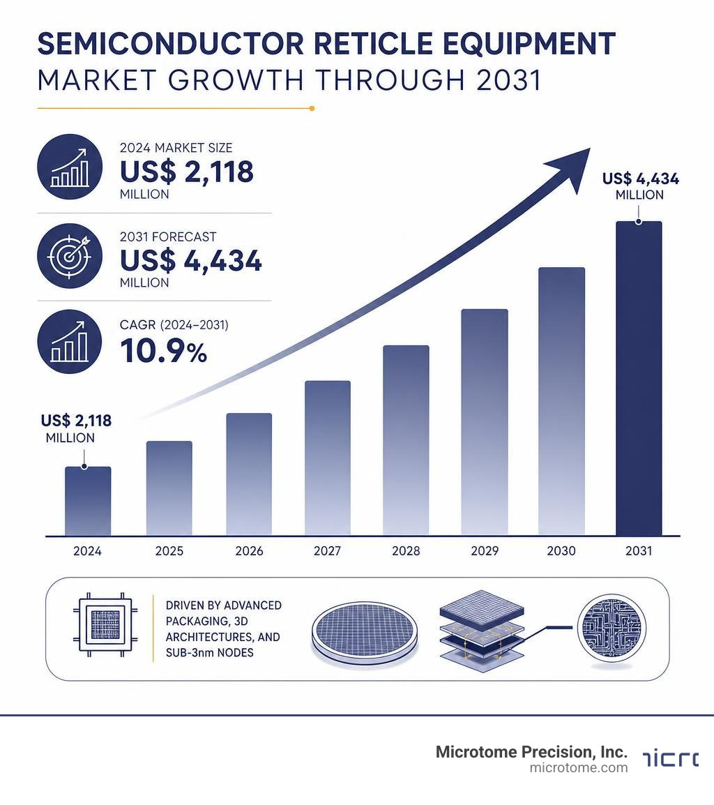
The demand for high-precision reticle fab equipment is growing rapidly, driven by the global transition to advanced packaging, 3D architectures, and sub-3nm nodes.
According to recent market research, the global market for Reticle Inspection and Metrology Equipment was valued at US$ 2,118 million in 2024 and is projected to reach US$ 4,434 million by 2031, growing at a compound annual growth rate (CAGR) of 10.9%.
To support this market growth, global production of these high-precision machines is expected to rise from 187 units in 2024 to over 356 units by 2031. Because of the extreme precision and proprietary technology required to build these tools, the industry maintains high gross profit margins of 40% to 60%.
Furthermore, this market is highly consolidated, with the top 5 companies holding more than 90% of the market share. While the Asia-Pacific (APAC) region continues to lead growth due to massive fab expansions, strict compliance with international SEMI standards remains a global requirement for any manufacturer entering this space. For historical context on the early modeling of EUV reticle manufacturing costs and factory yields, see the classic study UCRL-JC-123011 .
Frequently Asked Questions about Reticle Fab Equipment
What is reticle fab equipment and why is it critical?
Reticle fab equipment refers to the suite of tools used to write, inspect, measure, transport, and store photolithography masks. It is critical because reticles are the master templates for chip manufacturing. Any defect or contamination on a reticle will be repeatedly printed onto thousands of wafers, leading to catastrophic yield loss.
How do automated logistics reduce contamination risks?
Automated logistics systems (like AMRs and linear stockers) remove human operators from the handling loop. This eliminates the primary source of cleanroom particles and physical handling damage. Additionally, automated stockers utilize continuous nitrogen purging to prevent chemical outgassing and haze formation on the reticle surface.
What are the benefits of all-metal reticle pods?
All-metal reticle pods provide a physical Faraday cage that shields the reticle from external electric fields. This prevents Electric Field induced Migration (EFM) and Electrostatic Attraction (ESA) of particles, both of which are common causes of yield loss in standard plastic carriers.
Conclusion
Maximizing photolithography yield requires a holistic approach to reticle management. From advanced optical inspection tools and e-beam writers to automated logistics and Faraday-cage carrier protection, every piece of reticle fab equipment must work in perfect harmony.
At Microtome Precision, Inc., Reticle Protection is Our Business. Based in Colorado Springs, Colorado, we have spent nearly four decades designing and manufacturing the world’s most reliable, SEMI-compliant, all-metal reticle carriers to protect your multi-million dollar mask assets from electrostatic and particle contamination.
To learn more about our custom engineering capabilities, follow us on Microtome Precision Inc | LinkedIn or visit our Support and Repair page to keep your fleet operating at peak performance.