
The Definitive Guide to Comparing Advanced SMIF Pods
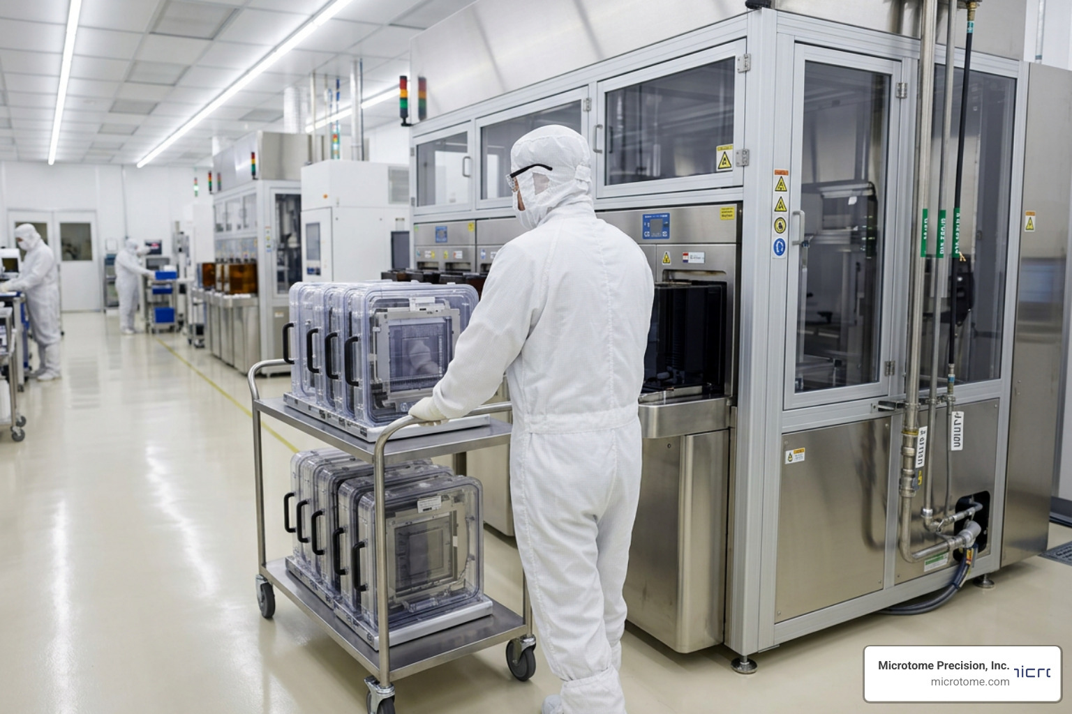
Why Advanced SMIF Pods Are Critical for Reticle Protection
Advanced SMIF pods are specialized enclosures that protect semiconductor wafers and reticles from contamination, mechanical damage, and electrostatic hazards during storage, transport, and processing in cleanroom environments.
Quick answer — what separates advanced SMIF pods from standard ones:
- Contamination control — maintain ISO Class 1 mini-environments around wafers and reticles
- Electrostatic protection — all-metal designs provide Faraday-cage shielding against EFM (Electric Field induced Migration), a failure mode that standard conductive plastics cannot fully address
- SEMI standards compliance — engineered to meet SEMI E100, E111, E112, and related standards for reticle and wafer handling
- Automation compatibility — designed to integrate with modern AMHS and Industry 4.0 fab systems
- Material choice matters — polymer vs. all-metal construction creates fundamentally different levels of electrostatic and contamination protection
Reticles are among the most expensive and irreplaceable components in semiconductor manufacturing. A single reticle can cost over a million dollars and take weeks to qualify. Yet many fabs still transport and store them in pods that leave them exposed to EFM — a low-level electrostatic failure mode that standard ESD controls simply weren’t designed to catch.
That gap between perceived protection and actual protection is what this guide addresses.
The global SMIF pod market is growing steadily, projected to reach $0.7 billion by 2034. But market size alone doesn’t tell you which pod design keeps your reticles safe at 3nm nodes and below. This guide cuts through the specs to show you what actually matters.
I’m Matt Pilarski, President of Microtome Precision, Inc., the longest-established independent designer and manufacturer of reticle carriers in the semiconductor industry — with direct experience shaping the SEMI standards that govern advanced SMIF pods since 1989. In the sections that follow, I’ll walk you through every factor that should drive your pod selection decisions.
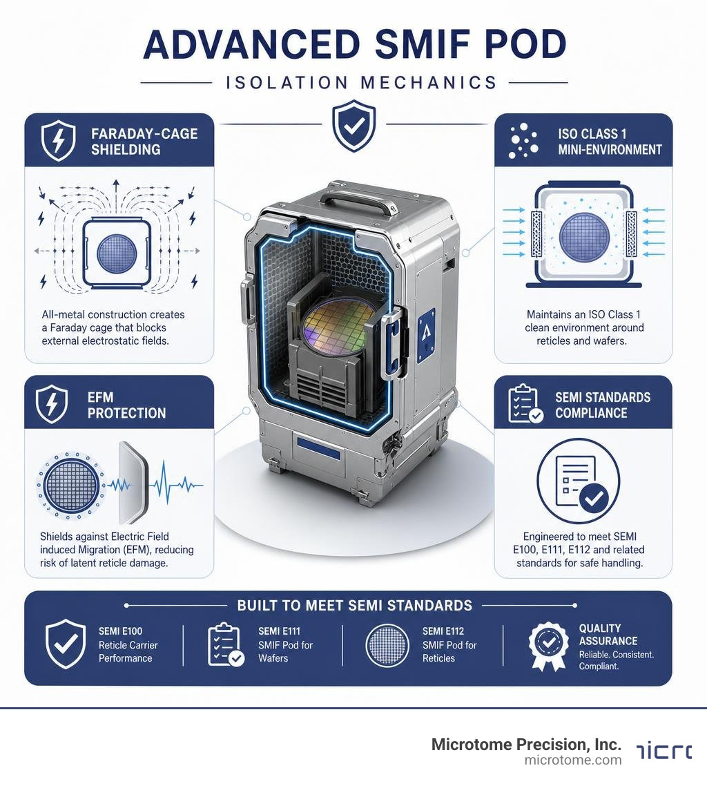
What is a SMIF Pod and Why is it Essential in Semiconductor Manufacturing?
A Standard Mechanical Interface (SMIF) pod is a sealed, transportable container designed to isolate critical semiconductor components—primarily wafers and photolithography reticles—from the ambient cleanroom environment. In modern fabrication facilities, the cleanroom itself is rarely clean enough to protect sub-micron features. Instead, fabs rely on a “mini-environment” strategy.
By keeping wafers and reticles inside an ISO Class 1 mini-environment, we can dramatically reduce the cost of keeping the entire ballroom cleanroom at an ultra-stringent specification. The SMIF pod serves as the mobile vault of this mini-environment.
When an advanced SMIF pod docks with a process tool, a specialized mechanism—such as an advanced SMIF pod opener—unlocks and lowers the pod door. The wafers or reticles are then transferred directly into the tool’s internal mini-environment without ever exposing them to external air.
While particle contamination prevention has always been the primary job of a reticle SMIF pod, advanced nodes have introduced a more insidious threat: Electrostatic Field-induced Migration (EFM). When electrostatic charges build up on a polymer pod shell, they generate electric fields. These fields pass right through plastic, attracting airborne molecular contaminants (AMCs) and sub-micron particles directly onto the active surface of the reticle.
To mitigate this, advanced semiconductor manufacturing requires robust electrostatic field mitigation (EFM). This is where all-metal SMIF pods shine, providing true Faraday-cage shielding that blocks external electric fields entirely, ensuring absolute yield optimization.
Material Science: Polymer vs. All-Metal in Advanced SMIF Pods
The choice of material for your advanced smif pods dictates their lifetime, contamination profile, and level of electrostatic protection.
Polycarbonate vs. Polypropylene SMIF Pods
Historically, polymer-based pods have dominated the market, with polycarbonate-based SMIF pods holding a 52.1% market share in 2025 (valued at $0.208 billion). Polycarbonate is widely preferred over polypropylene alternatives because it offers:
- Superior dimensional stability: Polycarbonate maintains tight physical tolerances under cleanroom temperature cycles, which is critical for automated robotic handling.
- Optical clarity: Allowing operators and automated sensors to visually inspect the contents or detect reticle presence.
- Chemical resistance: Excellent durability when exposed to standard cleanroom cleaning agents.
Polypropylene, by contrast, is softer, prone to warping under mechanical stress, and has a higher rate of particulate shedding due to wear. However, even high-purity polycarbonate has a fundamental limitation: it is an electrical insulator. Even when doped with carbon or static-dissipative additives, polymers cannot provide complete electromagnetic shielding.
The All-Metal Advantage: True Faraday-Cage Protection
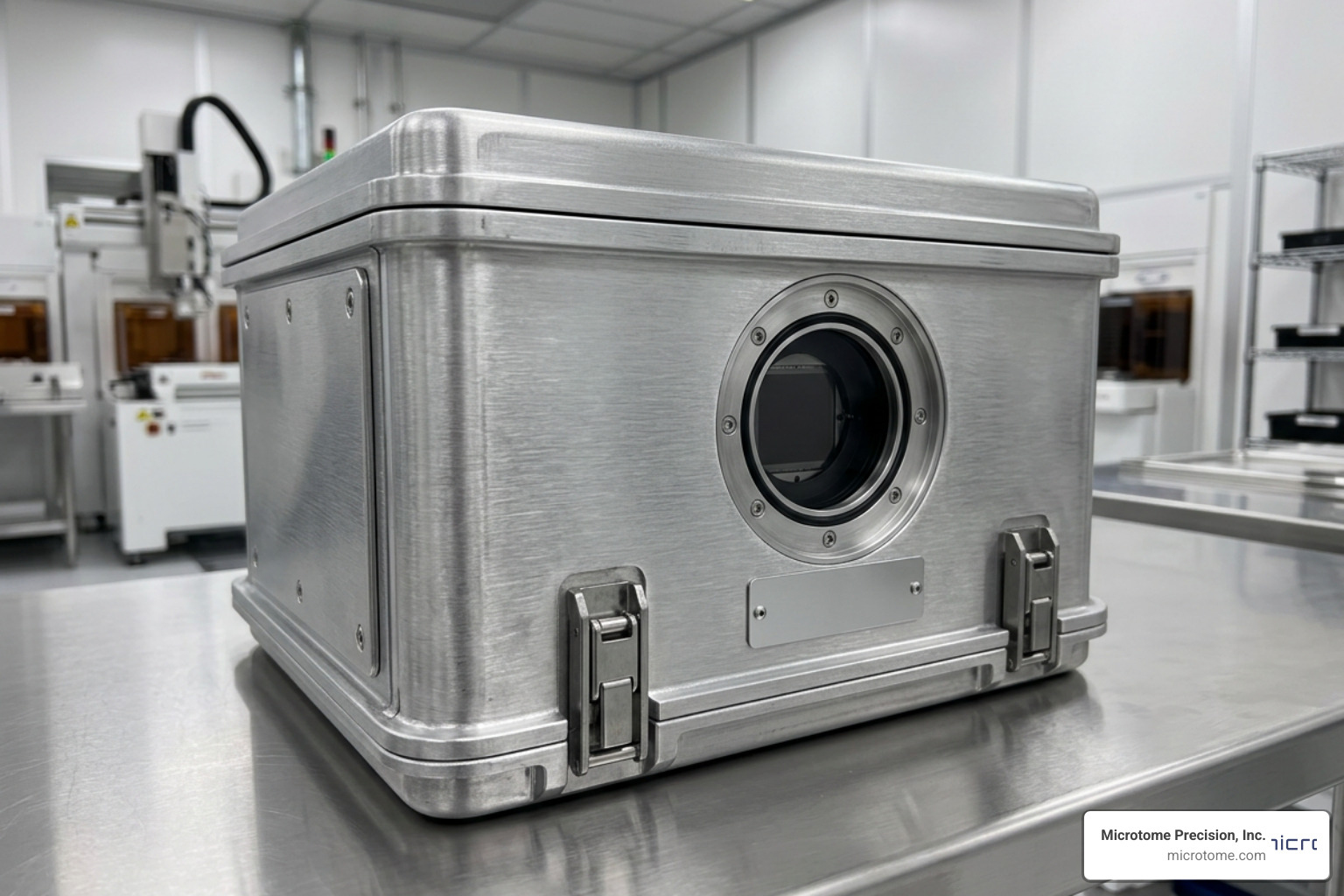
At Microtome Precision, we design and manufacture all-metal reticle SMIF pods at our facility in Colorado Springs, Colorado. Our proprietary research shows that only an all-metal construction provides a true Faraday cage.
When an electrostatic charge accumulates on the outside of an all-metal pod, the charge redistributes entirely along the outer conductive surface. The electric field inside the pod remains exactly zero. This completely eliminates EFM, preventing electrostatic fields from pulling microscopic contaminants onto your reticles.
Additionally, all-metal pods exhibit zero outgassing, superior dimensional stability over decades of operation, and are completely impervious to the chemical degradation that limits the lifespan of plastic pods.
Material Performance Comparison
| Feature / Metric | Polypropylene | Polycarbonate (ESD-Doped) | Microtome All-Metal (Aluminum/Nickel) |
|---|---|---|---|
| EFM Shielding (Faraday Cage) | None | Poor to Moderate | Excellent (Absolute) |
| Dimensional Stability | Low (Prone to warping) | Moderate to High | Excellent (Zero deformation) |
| Outgassing Profile | Moderate | Low | Zero |
| Durability & Lifespan | Low | Moderate | Extremely High |
| Cleanroom Cleanliness | ISO Class 3-5 | ISO Class 1-2 | ISO Class 1 (Zero shedding) |
Standard vs. Customized SMIF Pods: Market Demand and Reticle Size Dynamics
The semiconductor industry relies heavily on standardization to keep equipment costs manageable. However, the unique demands of proprietary process nodes and specialized substrates have split the market between standard and customized solutions.
Market Trends for Standard and Customized Advanced SMIF Pods
In 2025, standard SMIF pods held the largest market share at 58.2%, primarily driven by high-volume 200mm and 300mm silicon wafer lines that comply strictly with SEMI standards such as SEMI E100 (for physical interfaces) and SEMI E111 (for single reticle SMIF pods).
However, customized SMIF pods, which held 41.8% of the market in 2025, are growing at a faster rate—projected at a 6.8% CAGR through 2034 compared to 5.4% for standard pods. This rapid growth is driven by fabs implementing proprietary process nodes, advanced packaging configurations, and specialized manufacturing lines where standard plastic carriers fail to protect yields.
How Reticle Size and Node Migration Impact Advanced SMIF Pods
As fabs migrate to sub-3nm nodes, the physical and electrostatic tolerances of reticle carriers become incredibly tight. While wafer sizes have migrated to 300mm (representing 48.5% of the SMIF pod market value in 2025 at $0.194 billion), the standard photolithography reticle has stabilized around the 6-inch format.
At sub-3nm nodes, the introduction of Extreme Ultraviolet (EUV) lithography has changed the rules of reticle protection. EUV reticles do not use a protective pellicle in the same way deep ultraviolet (DUV) reticles do. Any particle that lands on an EUV reticle will print directly onto the silicon wafer.
Consequently, EUV and advanced DUV photolithography require reticle carriers with flawless dimensional stability and absolute EFM shielding. To ensure your tooling remains fully compatible across these evolving standards, you can View reticle carrier tool compatibility to see how our precision metal carriers interface with major lithography platforms.
Industry 4.0, Automation, and Emerging Fab Technologies
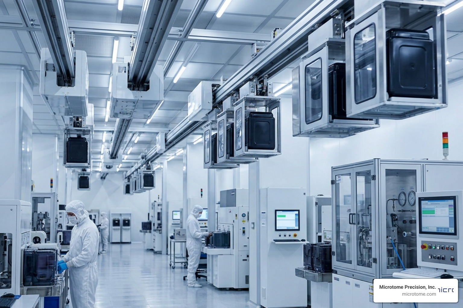
Modern semiconductor fabs are marvels of automation. In an Industry 4.0 environment, manual handling of reticle carriers is virtually non-existent. Instead, Automated Material Handling Systems (AMHS) and Overhead Hoist Transports (OHT) move SMIF pods seamlessly between storage stockers and tool load ports.
To support this level of automation, advanced smif pods must be “smart.” This is achieved by integrating:
- RFID tags and barcoding: To allow real-time tracking of reticle inventory and location throughout the fab.
- Smart sensors: To monitor internal humidity, temperature, and mechanical shock during transport.
- Purge systems: Allowing the pod to be flushed with ultra-pure nitrogen ($N_2$) or clean dry air (CDA) to prevent chemical reactions on the reticle surface.
Just as optimization algorithms in other industries streamline workflows—such as how publishers earn more from video content—automated fab dispatch systems utilize real-time data from smart SMIF pods to optimize lithography tool queues and minimize idle times.
Photonics vs. Semiconductor Manufacturing Requirements
While semiconductor manufacturing dominates the SMIF pod market (holding a 62.5% revenue share in 2025), photonics manufacturing is an emerging driver with distinct requirements.
Photonics devices, often built on compound semiconductors like III-V materials (GaAs, InP), are highly sensitive to specific optical and chemical contaminants. SMIF pods used in photonics require:
- Specialized chemical compatibility to handle non-silicon outgassing.
- Tight mechanical tolerances for handling delicate, non-standard substrate shapes.
- Enhanced ESD protection, as compound semiconductors typically have lower electrostatic breakdown voltages than silicon.
IDM vs. Foundry Procurement Strategies
Integrated Device Manufacturers (IDMs) and pure-play foundries approach SMIF pod procurement differently. IDMs represented the largest end-user segment in 2025 with a 39.2% market share ($0.157 billion). Because IDMs design and manufacture their own chips, they often prioritize customized, highly specialized SMIF pod solutions optimized for their proprietary, captive process flows.
Foundries, on the other hand, operate on a high-volume, multi-customer model. They place a premium on standard, highly compatible SMIF pods that can seamlessly transition between different customer runs and interface reliably with standard Support and Repair workflows.
Regardless of whether you are an IDM or a foundry, maintaining your carrier fleet is critical. Fabs rely on specialized Pod Repair services to re-certify worn mechanical components, seals, and kinematic coupling surfaces to prevent costly automation jams.
Frequently Asked Questions about Reticle Isolation
Why do manufacturers prefer all-metal over polymer for advanced SMIF pods?
While polymer pods made of polycarbonate are lighter, all-metal pods provide absolute Faraday-cage shielding. This blocks electrostatic fields (EFM) from reaching the reticle, preventing electrostatic damage and particle attraction. All-metal pods also offer zero outgassing, superior physical durability, and do not warp over decades of cleanroom service.
How do sub-3nm nodes affect reticle carrier specifications?
At sub-3nm nodes, particularly with EUV lithography, even a single sub-micron particle or chemical stain on a reticle can ruin wafer yields. This requires reticle carriers with near-zero particulate shedding, integrated nitrogen purging, and flawless EFM shielding to prevent airborne molecular contaminants from adhering to the reticle.
What role does automation play in modern carrier design?
Modern carriers must comply perfectly with SEMI standards (such as SEMI E100 and E111) to allow automated robotic grippers, OHT systems, and load ports to handle them without error. They must also integrate smart features like RFID tags for real-time inventory tracking within the fab’s Manufacturing Execution System (MES).
Conclusion
As the semiconductor industry pushes past the physical limits of silicon and scales down to sub-3nm nodes, the equipment protecting your most valuable assets must evolve. Standard plastic pods, while sufficient for legacy nodes, expose modern high-value reticles to the costly risks of EFM and chemical degradation.
At Microtome Precision, Inc., we have spent decades perfecting the physics of reticle protection. From our headquarters in Colorado Springs, Colorado, we design and manufacture all-metal advanced smif pods that provide unmatched Faraday-cage shielding, zero outgassing, and rugged, automation-ready reliability.
Just as specialized formulas in other fields are engineered for highly sensitive environments—much like how SMA® ADVANCED Follow-on Milk Powder is developed for specific developmental needs—our all-metal pod metallurgy is custom-engineered to protect the delicate, multi-million dollar reticles that drive the future of technology.
Protect your yields and eliminate electrostatic migration risks today. Consult with our electrostatic protection experts to evaluate your fab’s current ESD profile, or Explore our full product catalog to find the perfect all-metal carrier solution for your lithography tools.